Apparatus and methods for plug fill deposition in 3-d NAND applications

a technology of notand and plug fill, which is applied in the direction of solid-state devices, chemical vapor deposition coatings, coatings, etc., can solve the problems of inability to meet the requirements of the application, the time between the liner b>160/b> and the plug fill b>170/b> may be undesirably long, and the stack may be misaligned

Active Publication Date: 2020-08-20
ASM IP HLDG BV
View PDF0 Cites 169 Cited by
  • Summary
  • Abstract
  • Description
  • Claims
  • Application Information

AI Technical Summary

Benefits of technology

[0012]This summary is provided to introduce a selection of concepts in a simplified form. These concepts are described in further detail in the detailed description of example embodiments of the disc

Problems solved by technology

Depending on the material used for the plug fill 170, there may be increased cost and a greater risk of instability due to failure as it relates to integration.
In addition, the removal of the liner 160 and the plug fill 170 may be done with a slow etch rate, whic

Method used


Image

  • Apparatus and methods for plug fill deposition in 3-d NAND applications
  • Apparatus and methods for plug fill deposition in 3-d NAND applications
  • Apparatus and methods for plug fill deposition in 3-d NAND applications

Examples


Embodiment Construction

[0020]Although certain embodiments and examples are disclosed below, it will be understood by those in the art that the invention extends beyond the specifically disclosed embodiments and / or uses of the invention and obvious modifications and equivalents thereof. Thus, it is intended that the scope of the invention disclosed should not be limited by the particular disclosed embodiments described below.

[0021]The illustrations presented herein are not meant to be actual views of any particular material, structure, or device, but are merely idealized representations that are used to describe embodiments of the disclosure.

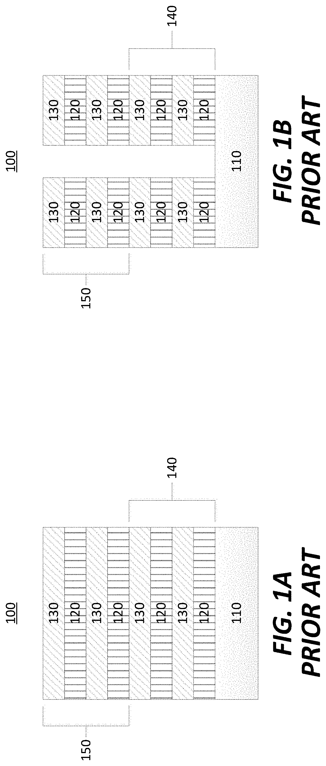
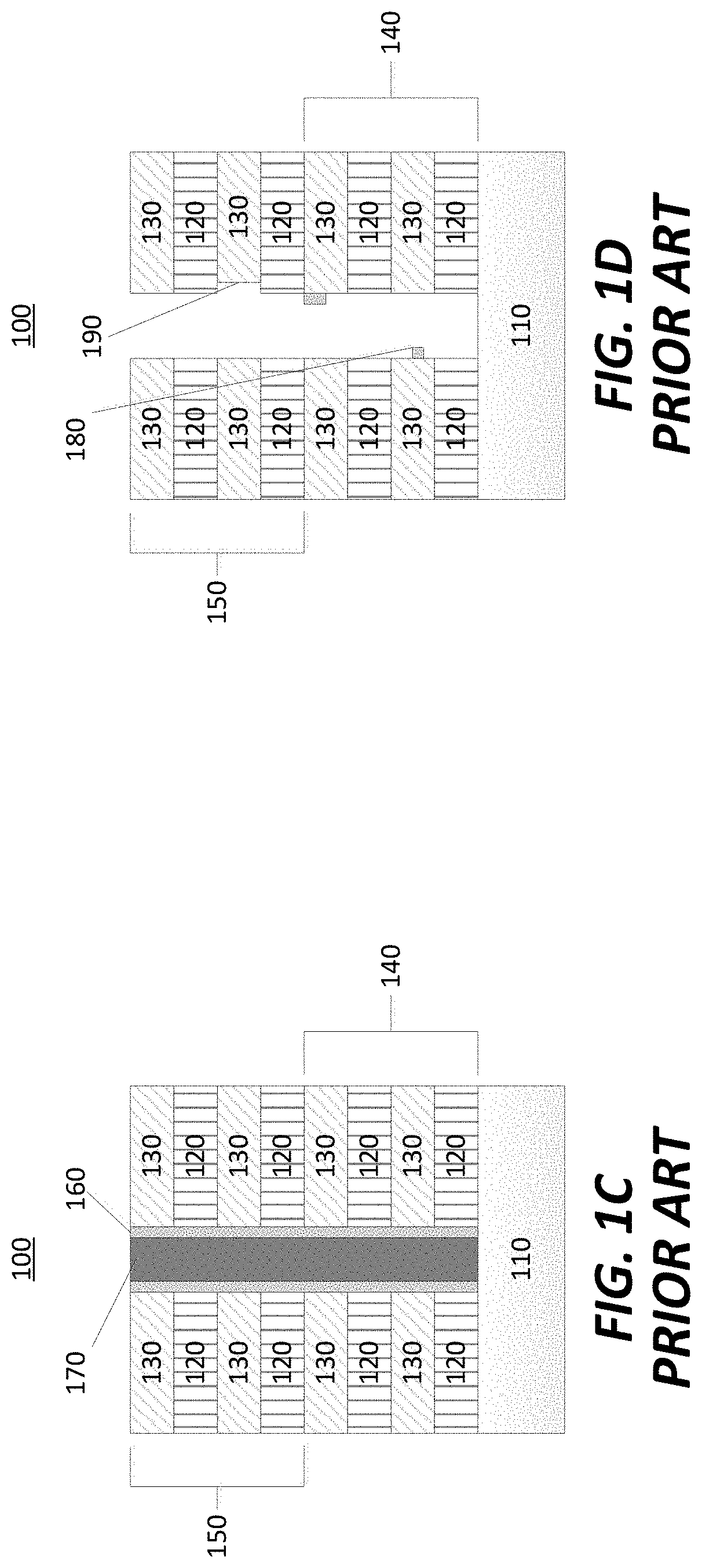
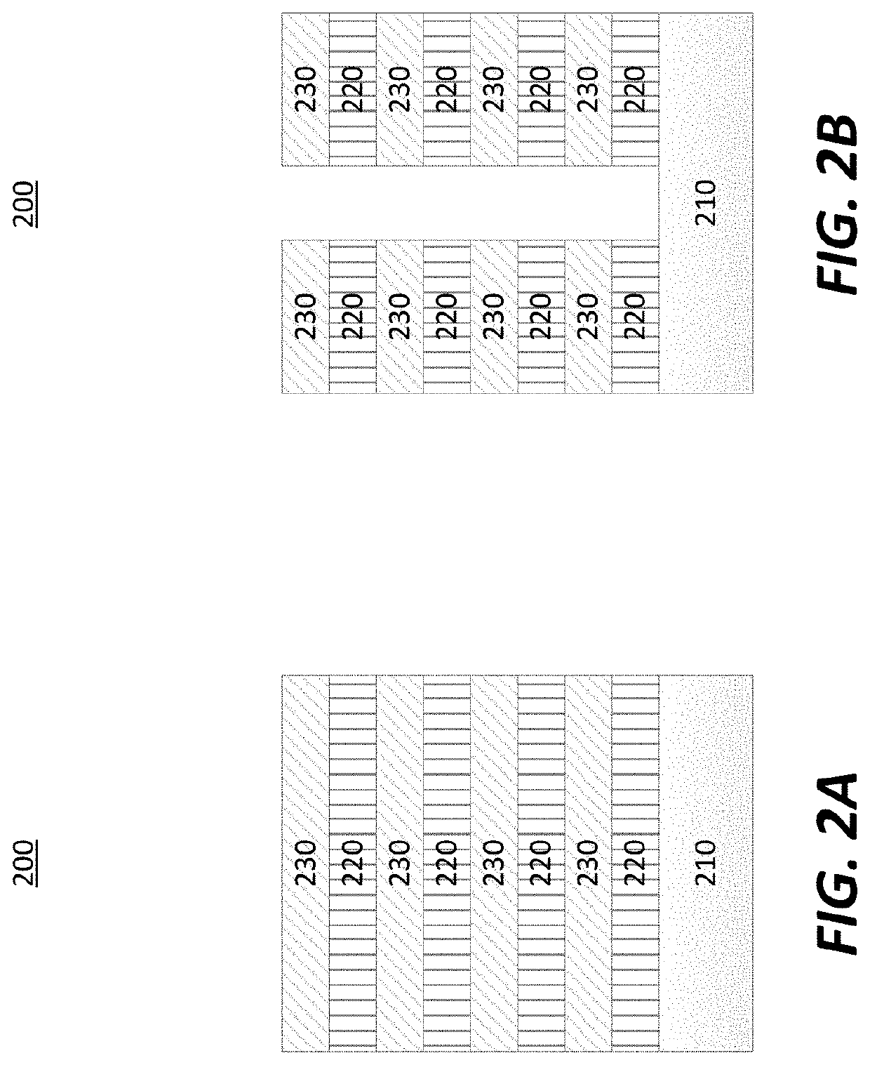
[0022]Three-dimensional (3-D) Not-AND (NAND) devices may be utilized in memory applications. The 3-D NAND devices may involve stacks of bilayers disposed on each other. The bilayers may comprise oxides and nitrides, for example. When disposing stacks of multiple bilayers on other stacks, alignment and stresses on the layers and different features may become critical.

[0...


PUM

PropertyMeasurementUnit
Fractionaaaaaaaaaa
Fractionaaaaaaaaaa
Sizeaaaaaaaaaa

Abstract

An apparatus and a method for forming a 3-D NAND device are disclosed. The method of forming the 3-D NAND device may include forming a plug fill and a void. Advantages gained by the apparatus and method may include a lower cost, a higher throughput, little to no contamination of the device, little to no damage during etching steps, and structural integrity to ensure formation of a proper stack of oxide-nitride bilayers.

Description

CROSS-REFERENCE TO RELATED APPLICATIONS[0001]This application is a nonprovisional of, and claims priority to and the benefit of, U.S. Provisional Patent Application Ser. No. 62 / 807,989, filed Feb. 20, 2019 and entitled, “APPARATUS AND METHODS FOR PLUG FILL DEPOSITION IN 3-D NAND APPLICATIONS,” which is hereby incorporated by reference.FIELD OF INVENTION[0002]The present disclosure generally relates to an apparatus and methods for forming Not-AND (NAND) Devices. More particularly, the disclosure relates to deposition of a plug fill for a 3-D NAND device made in part of oxide-nitride layer stacks. The apparatus and method for forming the NAND devices may include use of a sacrificial material and fabrication scheme to achieve proper formation of device structures at lower cost and higher throughput.BACKGROUND OF THE DISCLOSURE[0003]NAND devices are logic gates usable in applications such as flash memory, for example. Manufacture of the NAND devices may include formation of a channel ho...

Claims


Application Information

Patent Timeline
IPC IPC(8): H01L27/11582H01L27/11556H01L21/02H01L21/311H01L21/306
CPCH01L21/30625H01L21/02532H01L21/0217H01L21/31116H01L27/11556H01L21/02579H01L21/02576H01L27/11582H01L21/02164H01L21/022H01L21/76898H10B41/41H10B41/42H10B41/35H10B41/27H10B43/40H10B43/35H10B43/27H01L21/31111H01L21/0262H01L21/02439H01L21/76802C23C16/045H01L21/02664
Inventor KIM, BOKHEONKOHEN, DAVIDDEMOS, ALEXANDROS
Owner ASM IP HLDG BV
Why Eureka
Try Eureka