Supercharge Your Innovation With Domain-Expert AI Agents!

Photoelectric conversion apparatus, photoelectric conversion system, and moving object

a technology of photoelectric conversion and conversion system, applied in the direction of scene recognition, radio frequency controlled devices, instruments, etc., can solve problems such as the difficulty of conducting a layout study, and achieve the effect of high diode integration

Active Publication Date: 2020-08-27
CANON KK
View PDF0 Cites 1 Cited by
  • Summary
  • Abstract
  • Description
  • Claims
  • Application Information

AI Technical Summary

Benefits of technology

The present patent is about improving the performance of a photoelectric conversion device by integrating diodes with a quench element that includes a transistor. This combination of elements allows for more efficient and effective operation of the device.

Problems solved by technology

However, United States Patent Publication Application No. 2015 / 0115131 fails to conduct a study on a layout of the quench element and the diode when the diode and the quench element are mixed in the same substrate.

Method used

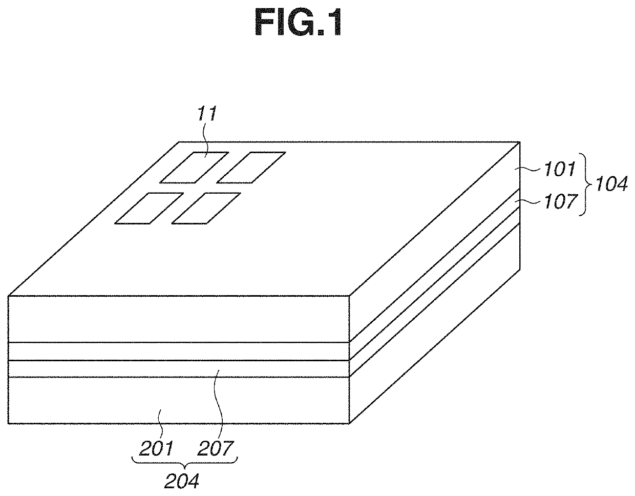
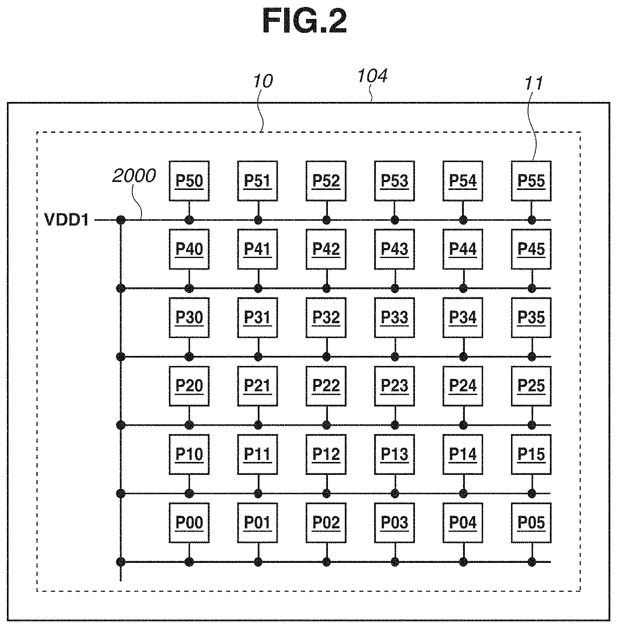
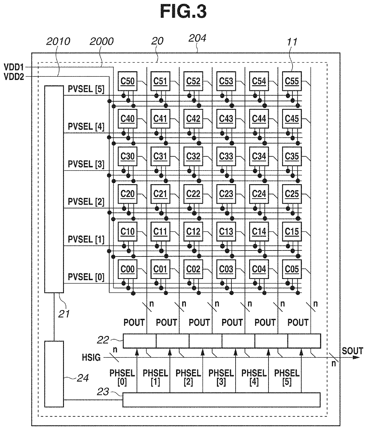

Image

  • Photoelectric conversion apparatus, photoelectric conversion system, and moving object
  • Photoelectric conversion apparatus, photoelectric conversion system, and moving object
  • Photoelectric conversion apparatus, photoelectric conversion system, and moving object

Examples


second exemplary embodiment

(Exemplary Modification of Second Exemplary Embodiment)

[0088]FIG. 10 illustrates another layout example of the above-described diode 12, well region 114, and well region 117. The power source lines are omitted in FIG. 10.

[0089]The well region 114 and the well region 117 illustrated in FIG. 10 are arranged so as to be rotated by 45 degrees in the row and column directions. In other words, the boundary line with the element isolation region 113 disposed between the first diode and the well region 114 perpendicularly intersects with the line connecting the first diode and the second diode in the planar view. By employing such a layout, the present exemplary embodiment can reduce the distance from the center of the semiconductor region 111 of the diode 12 to the well region 114 compared to a case where the well region 114 and the well region 117 are not rotated by 45 degrees in the row and column directions. In other words, the present exemplary embodiment can achieve the high integrati...


PUM

PropertyMeasurementUnit
power source voltageaaaaaaaaaa
voltageaaaaaaaaaa

Abstract

A photoelectric conversion apparatus includes a first diode which is an avalanche multiplication-type and a second diode which is an avalanche multiplication-type formed within a semiconductor substrate, a first transistor forming a first quench element, and a second transistor forming a second quench element. The first transistor and the second transistor are disposed between the first diode and the second diode in a planar view. The first transistor and the second transistor are disposed in a common semiconductor well region formed within the semiconductor substrate.

Description

BACKGROUND OF THE INVENTIONField of the Invention[0001]The present disclosure relates to a photoelectric conversion apparatus, a photoelectric conversion system, and a moving object.Description of the Related Art[0002]Conventionally, there a photoelectric conversion apparatus has been known that includes a single photon avalanche diode (SPAD). The SPAD is an element that counts the number of incident photons by detecting an avalanche current that has occurred due to entry of a single photon to an avalanche photodiode (hereinafter referred to as a diode). A reverse bias voltage equal to or higher than a breakdown voltage is applied to the diode, and the current is multiplied due to the avalanche multiplication. A photoelectric conversion apparatus including the SPAD counts the number of times that the current multiplied in the avalanche multiplication (hereinafter referred to as the “avalanche current”) exceeds a threshold value.[0003]United States Patent Publication Application No. ...

Claims


Application Information

Patent Timeline
Patent Type & Authority Applications(United States)
IPC IPC(8): H01L27/146G06K9/00
CPCH01L27/14645G06K2209/21H01L27/14607G06K9/00805H01L27/14612H01L27/1463H01L27/14627H01L27/14621H01L27/1464H01L27/1461H01L27/14634H01L27/14636H04N25/773G06V20/58G06V2201/07
Inventor SASAGO, TOMOYAKURODA, YUKIHIRO
Owner CANON KK
Features
  • R&D
  • Intellectual Property
  • Life Sciences
  • Materials
  • Tech Scout
  • Unparalleled Data Quality
  • Higher Quality Content
  • 60% Fewer Hallucinations
Learn More