

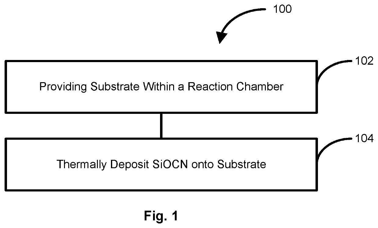
STRUCTURE INCLUDING SiOCN LAYER AND METHOD OF FORMING SAME
a technology of siocn layer and structure, applied in the direction of coating, chemical vapor deposition coating, metallic material coating process, etc., can solve the problems of high temperature not being suitable for some applications, high temperature being relatively high, and film formation using pecvd generally showing relatively high wet etch ra
- Summary
- Abstract
- Description
- Claims
- Application Information
AI Technical Summary
Benefits of technology
Problems solved by technology
Method used
Image

Examples
Embodiment Construction
[0013]Although certain embodiments and examples are disclosed below, it will be understood by those in the art that the invention extends beyond the specifically disclosed embodiments and / or uses of the invention and obvious modifications and equivalents thereof. Thus, it is intended that the scope of the invention disclosed should not be limited by the particular disclosed embodiments described below.
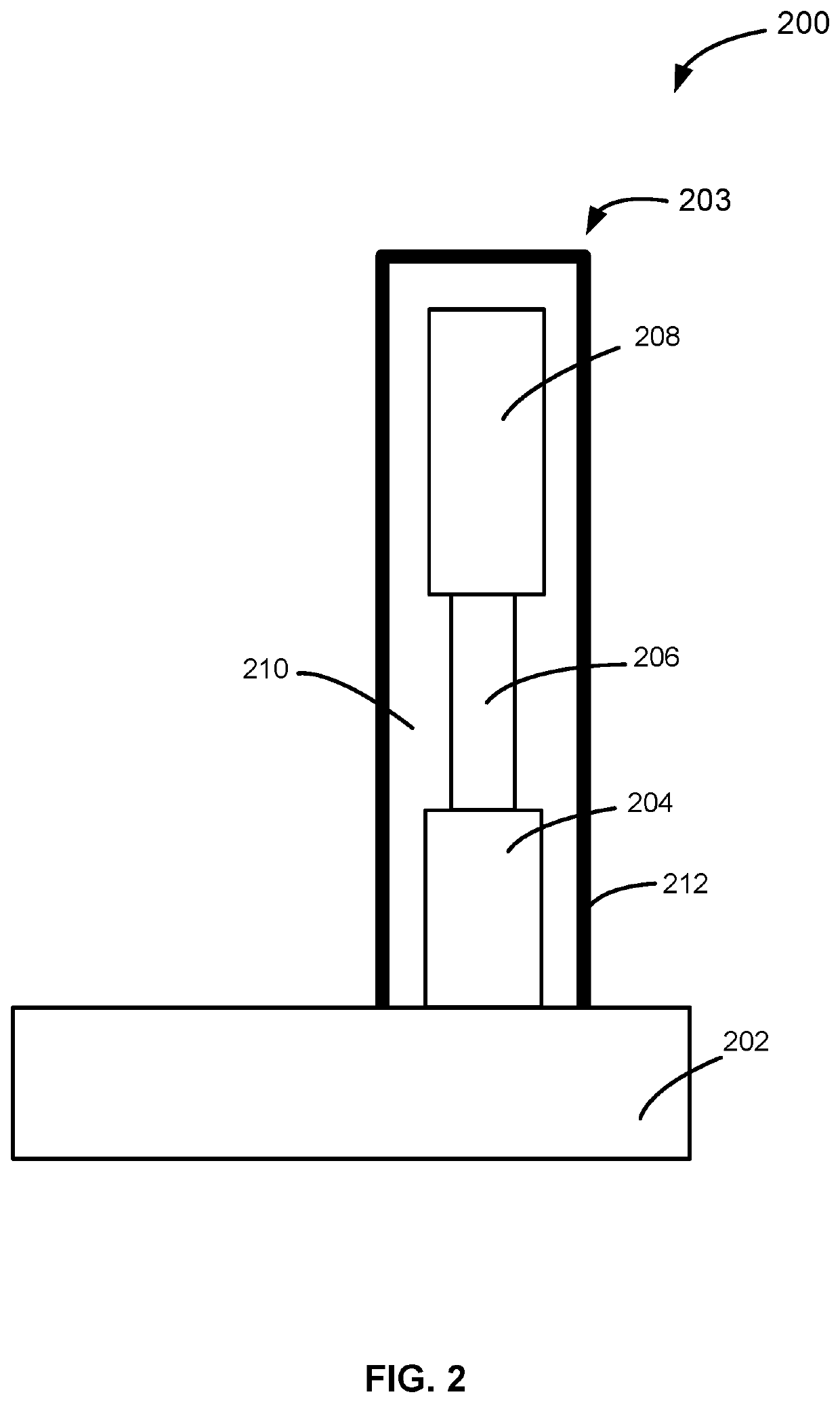
[0014]As used herein, the term “substrate” may refer to any underlying material or materials that may be used to form, or upon which, a device, a circuit, or a film may be formed. A substrate can include a bulk material, such as silicon (e.g., single-crystal silicon) and can include one or more layers overlying the bulk material. Further, the substrate can include various topologies, such as recesses, lines, and the like formed within or on at least a portion of a layer of the substrate.
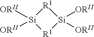
[0015]As used herein, the term “cyclical deposition” may refer to the sequential introduction of pre...
PUM
| Property | Measurement | Unit |
|---|---|---|
| temperature | aaaaa | aaaaa |
| temperature | aaaaa | aaaaa |
| pressure | aaaaa | aaaaa |
Abstract
Description
Claims
Application Information