
Oxy-fluoride compounds for chamber parts protection

a technology of oxyfluoride compounds and chamber parts, which is applied in the direction of coatings, chemical vapor deposition coatings, electric discharge tubes, etc., can solve the problems of oled, flat panel processing may corrode the surface of semiconductors, impact on product yield, chamber uptime, and customers' cos

Active Publication Date: 2020-09-10
APPLIED MATERIALS INC
View PDF0 Cites 2 Cited by
  • Summary
  • Abstract
  • Description
  • Claims
  • Application Information

AI Technical Summary

Benefits of technology

This patent provides methods for forming fluorinated metal films using atomic layer deposition (ALD) and activated fluorination processes. The methods involve depositing layers of metal-oxide and metal-fluorine onto an object using precursors containing organofluorine reagents or fluorinated gases. The resulting films have a high degree of purity and can be used in various applications such as electronics, optics, and sensors. The technical effects of this patent include improved methods for forming high-quality fluorinated metal films with precise control over film thickness and improved purity.

Problems solved by technology

Absent the fluorinated coating, halogenated plasma during semiconductor, OLED, and flat panel processing may corrode the surfaces of the semiconductor, OLED, and flat panel devices.
The corrosion of the surfaces that may be present could impact semiconductor, OLED, and flat panel performance and impact product yield, chamber uptime, and customers cost.
Most current fluorinating coating techniques utilize materials, such as HF-pyridine and fluorine, that do not provide precise control of properties of the fluorinated coating.

Method used


Image

  • Oxy-fluoride compounds for chamber parts protection
  • Oxy-fluoride compounds for chamber parts protection
  • Oxy-fluoride compounds for chamber parts protection

Examples


Embodiment Construction

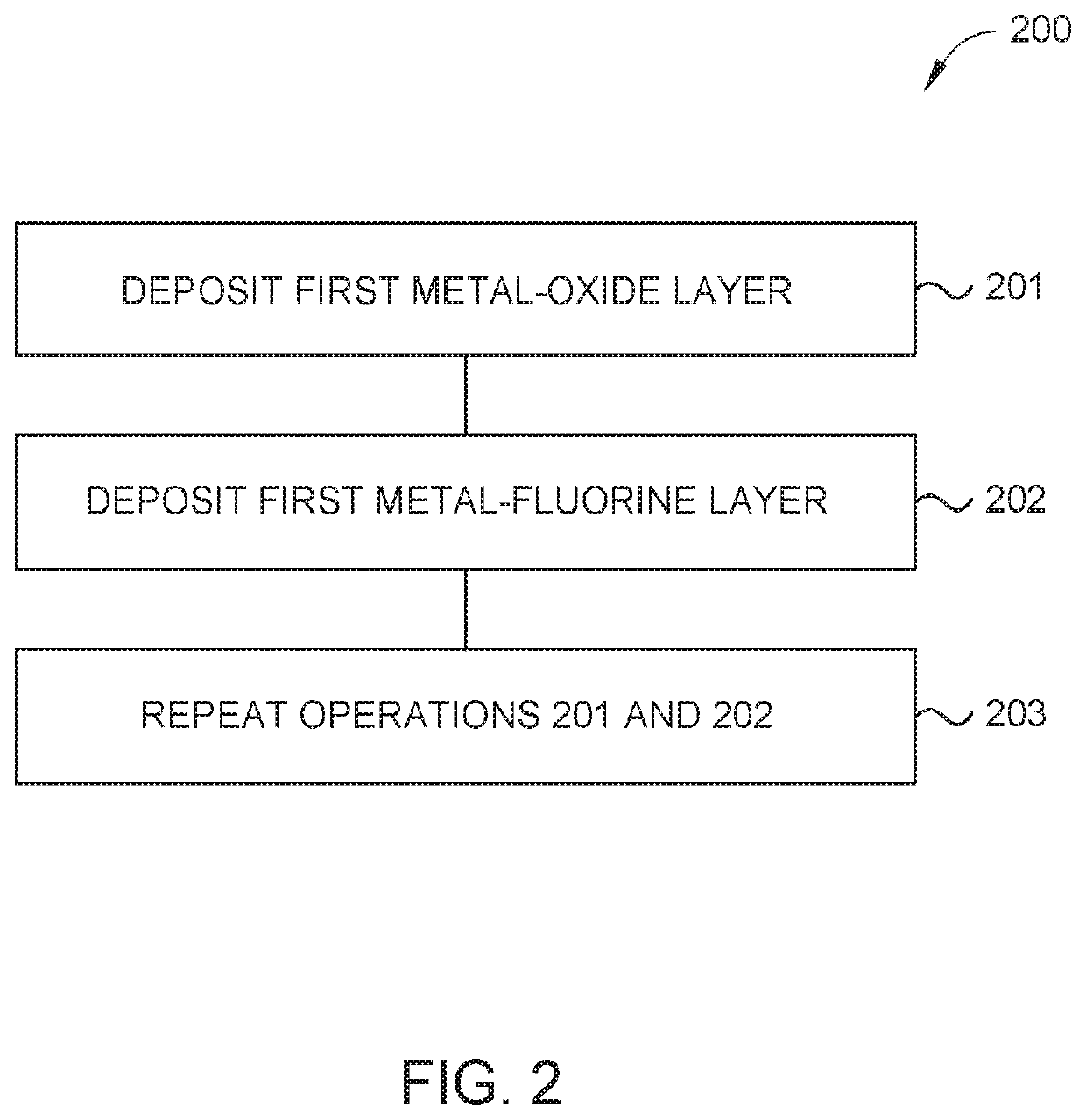
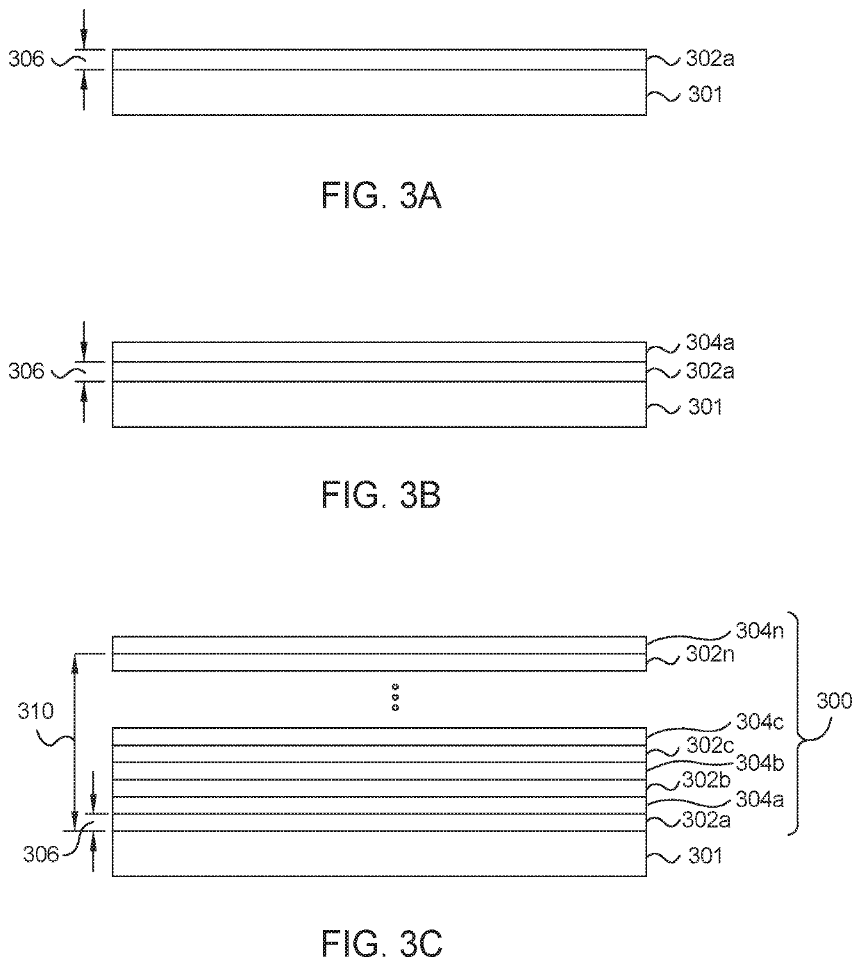
[0014]Embodiments described herein relate to a method of forming a fluorinated metal film. The method includes depositing a metal-oxide containing layer on an object using an atomic layer deposition (ALD) process, depositing a metal-fluorine layer on the metal-oxide containing layer using an activated fluorination process, and repeating depositing the metal-oxide containing layer and depositing the metal-oxide containing layer until a fluorinated metal film with a predetermined film thickness is formed.

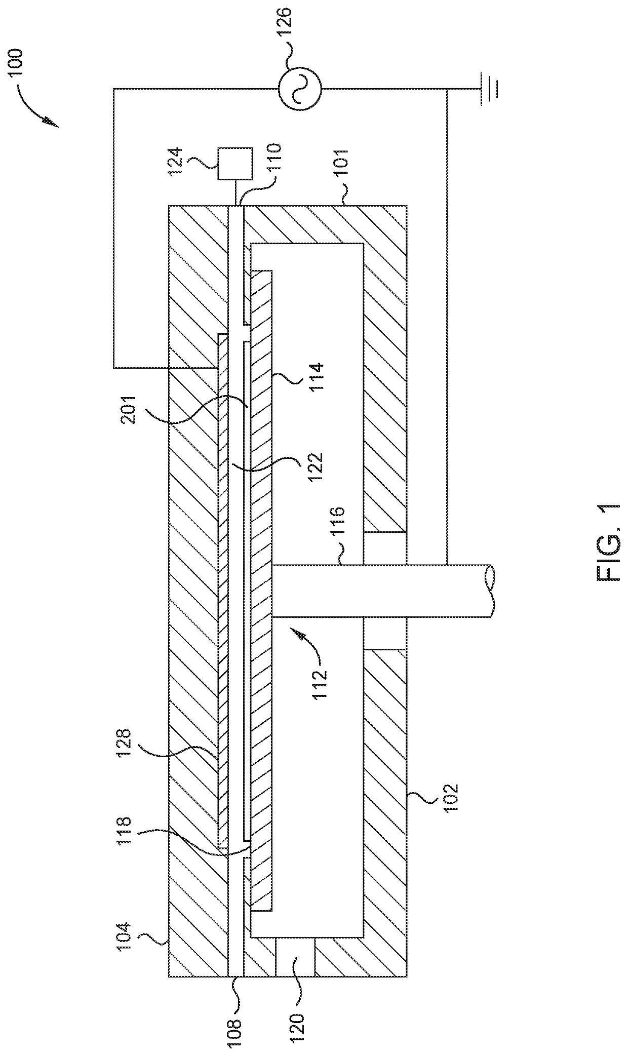
[0015]FIG. 1 is a schematic view of an atomic layer deposition (ALD) chamber 100. It is to be understood that the chamber described below is an exemplary chamber and other chambers, including chambers from other manufacturers, may be used with or modified to accomplish aspects of the present disclosure, such a method 200 of forming a fluorinated metal film 300.

[0016]The ALD chamber 100 includes a chamber body 101. The chamber body includes a body portion 102, and a lid portion 104, an...


PUM

PropertyMeasurementUnit
Thicknessaaaaaaaaaa

Abstract

Embodiments described herein provide a method of forming amorphous a fluorinated metal film. The method includes positioning an object in an atomic layer deposition (ALD) chamber having a processing region, depositing a metal-oxide containing layer on an object using an atomic layer deposition (ALD) process, depositing a metal-fluorine layer on the metal-oxide containing layer using an activated fluorination process, and repeating the depositing the metal-oxide containing layer and the depositing the metal-oxide containing layer until a fluorinated metal film with a predetermined film thickness is formed. The activated fluorination process includes introducing a first flow of a fluorine precursor (FP) to the processing region. The FP includes at least one organofluorine reagent or at least one fluorinated gas.

Description

CROSS-REFERENCE TO RELATED APPLICATIONS[0001]This application claims priority to U.S. Provisional Patent Application Ser. No. 62 / 813,512, filed on Mar. 4, 2019, which herein is incorporated by reference.BACKGROUNDField[0002]Embodiments of the present disclosure generally relate to a method of forming a fluorinated metal film. More particularly, embodiments of the present disclosure relate to coating components with the method of forming the fluorinated metal film.Description of the Related Art[0003]In the cleaning or manufacturing of semiconductor, OLED, and flat panel devices, such as substrates, chamber components, chamber tools, chambers, and chamber mainframes, it is often desirable to form a fluorinated coating on the devices. Absent the fluorinated coating, halogenated plasma during semiconductor, OLED, and flat panel processing may corrode the surfaces of the semiconductor, OLED, and flat panel devices. The corrosion of the surfaces that may be present could impact semiconduc...

Claims


Application Information

Patent Timeline
IPC IPC(8): C23C16/455C23C16/08C23C16/40C23C22/34
CPCC23C22/34C23C16/40C23C16/08C23C16/45536C23C16/45553C23C16/45529C23C16/4404C23C16/405C23C16/403C23C16/45534C23C16/30H01J37/32477
Inventor DEEPAK, NITINSETH, SURESH CHANDGORADIA, PRERNA SONTHALIABAJAJ, GEETIKATHAKARE, DARSHANSUN, JENNIFER Y.NATU, GAYATRI
Owner APPLIED MATERIALS INC
Learn More