System and Method for the Characterization and Dispersal of Emissive Elements

a technology of emissive elements and dispersible elements, applied in semiconductor/solid-state device testing/measurement, instruments, material analysis, etc., can solve the problems of image burn-in, limited contrast ratio, and less than 4% efficiency of lcd display, and achieve the effect of minimizing damage and loss of microleds

Active Publication Date: 2020-09-10
ELUX INC
View PDF0 Cites 1 Cited by
  • Summary
  • Abstract
  • Description
  • Claims
  • Application Information

AI Technical Summary

Benefits of technology

[0019]Described herein are systems and methods for formulating and manipulating a micro-light emitting diode (microLED) suspension that are suitable for the fluidic assembly of microLED displays. A selective harvest method produces a microLED suspension composed of known good LEDs at a well determined concentration in an appropriate liquid. The microLED suspension is supplied to the display substrate using a dispensing system which minimizes damage and loss of microLEDs while producing a uniform distribution of devices at a controlled density over the display substrate. This optimum initial condition is essential for successful fluidic assembly of microLED displays.

Problems solved by technology

As a consequence, the efficiency of an LCD display may be less than 4% and the contrast ratio is limited by light leaking through the cell.
The OLED materials are direct emitting so the display contrast ratio is high, but the organic materials can be subject to long term degradation causing image burn-in.
MicroLEDs are fabricated from metalorganic chemical vapor deposition (MOCVD) wafers like those used to make LEDs for general lighting, which makes the cost per device very low but also introduces some problems that are unique to the microLED technology.
That constraint has caused LED fabrication practices to use a process called binning to deal with process variability and defects.
These defects would cause a dark sub-pixel, which is not acceptable for a display product.
The microLED is not packaged and the very small size of the device, especially the electrodes, makes device handling and functional test difficult.
Therefore, the binning technique is not practical to identify and discard defective microLEDs.
It is possible to remove a defective microLED and replace it as has been described in parent application Ser. Nos. 16 / 125,671, 16 / 595,623, and 16 / 693,674, which are incorporated herein by reference, but the mechanical pick-and-place tools are expensive to buy and operate.
Unfortunately, the conventional techniques for suspension handling are not compatible with the properties of microLEDs or the requirements of the fluidic assembly technology.
MicroLEDs must settle to the target substrate surface for assembly to take place, so microLED suspensions for fluidic assembly generally settle completely in minutes and lose uniformity very quickly after cessation of mixing.
As such, it is nearly impossible to prevent temporary stiction to solid surfaces in contact with the microLED suspension.
A broken microLED is similar in major dimension to a good microLED, so it cannot be removed from the suspension by filtering, and it interferes with fluidic assembly by partially blocking a trap site.
MicroLEDs represent a large fraction of the cost to manufacture a display, and inefficiencies in μLED utilization and recapture strongly influence cost.

Method used


Image

  • System and Method for the Characterization and Dispersal of Emissive Elements
  • System and Method for the Characterization and Dispersal of Emissive Elements
  • System and Method for the Characterization and Dispersal of Emissive Elements

Examples


Embodiment Construction

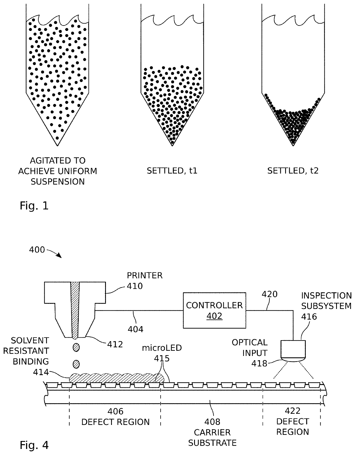
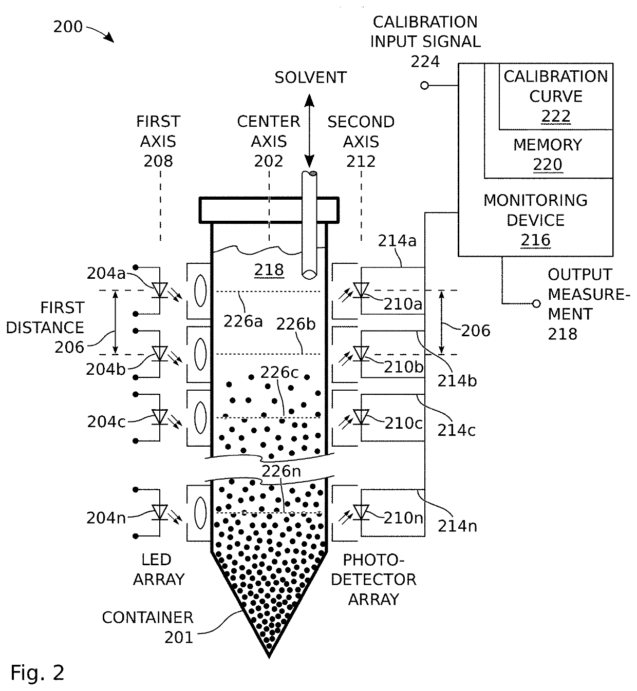
[0054]FIG. 2 is a partial cross-sectional view of a system for characterizing a micro-light emitting diode (microLED) suspension. The system 200 comprises a transparent container 201 having a vertical center axis 202. A plurality of light emitting devices 204a through 204n (LED array) is shown with each light emitting device having a predetermined output light intensity, directed towards the center axis 202 of the container 200 and spaced a first predetermined distance 206 from each other along a vertical first axis 208 parallel to the center axis 202, where (n) is an integer greater than 1. A plurality of light detection devices 210a through 210n (photodetector array) is spaced the first predetermined distance 206 from each other along a vertical second axis 212 parallel to the center axis 202. The light detection devices 210a-210n each have an optical input directed towards a corresponding light emitting device output and an output, respectively on lines 214a through 214n, to prov...


PUM

PropertyMeasurementUnit
sizeaaaaaaaaaa
diameteraaaaaaaaaa
diameteraaaaaaaaaa

Abstract

A method is provided for the selective harvest of microLED devices from a carrier substrate. Defect regions are predetermined that include a plurality of adjacent defective microLED devices on a carrier substrate. A solvent-resistant binding material is formed overlying the predetermined defect regions and exposed adhesive is dissolved with an adhesive dissolving solvent. Non-defective microLED devices located outside the predetermined defect regions are separated from the carrier substrate while adhesive attachment is maintained between the microLED devices inside the predetermined defect regions and the carrier substrate. Methods are also provided for the dispersal of microLED devices on an emissive display panel by initially optically measuring a suspension of microLEDs to determine suspension homogeneity and calculate the number of microLEDs per unit volume. If the number of harvested microLED devices in the suspension is known, a calculation can be made of the number of microLED devices per unit of suspension volume.

Description

RELATED APPLICATIONS[0001]Any and all applications, if any, for which a foreign or domestic priority claim is identified in the Application Data Sheet of the present application are hereby incorporated by reference under 37 CFR 1.57.BACKGROUND OF THE INVENTION1. Field of the Invention[0002]This invention generally relates to light emitting diodes (LEDs) having a size of less than 100 microns and, more particularly, to microLED fabrication processes and systems.2. Description of the Related Art[0003]A red / green / blue (RGB) display is composed of pixels that emit light at three wavelengths corresponding to the visible colors red, green, and blue. The RGB components of the pixel, each of which is referred to as a sub-pixel, are energized in a systematic way to additively produce the colors of the visible spectrum. There are several display types that produce the RGB images in different ways. Liquid crystal displays (LCD) are the most prevalent technology and they produce RGB images by s...

Claims


Application Information

Patent Timeline
Patent Type & Authority Applications(United States)
IPC IPC(8): H01L25/075H01L33/48H01L33/38
CPCH01L2933/0066H01L33/38H01L25/0753H01L2933/0033H01L33/486H01L21/6835H01L21/7806H01L22/22H01L23/544H01L33/0095H01L2221/68363H01L2221/68368H01L2221/68381H01L2223/54426H01L2223/54433H01L2223/5446H01L2223/54493H01L2224/95101H01L24/74G01N21/5907H01L2224/751G01N2021/5919H01L22/10H01L24/799
Inventor SASAKI, KENJIULMER, KURTSCHUELE, PAUL J.LEE, JONG-JAN
Owner ELUX INC
Why Eureka
Try Eureka