

System and Method for the Selective Harvest of Emissive Elements
a technology of selective harvesting and emissive elements, applied in semiconductor/solid-state device testing/measurement, instruments, material analysis, etc., can solve the problems of image burn-in, limited contrast ratio, and less than 4% efficiency of lcd display, and achieve the effect of minimizing damage and loss of microleds
- Summary
- Abstract
- Description
- Claims
- Application Information
AI Technical Summary
Benefits of technology
Problems solved by technology
Method used
Image

Examples
Embodiment Construction
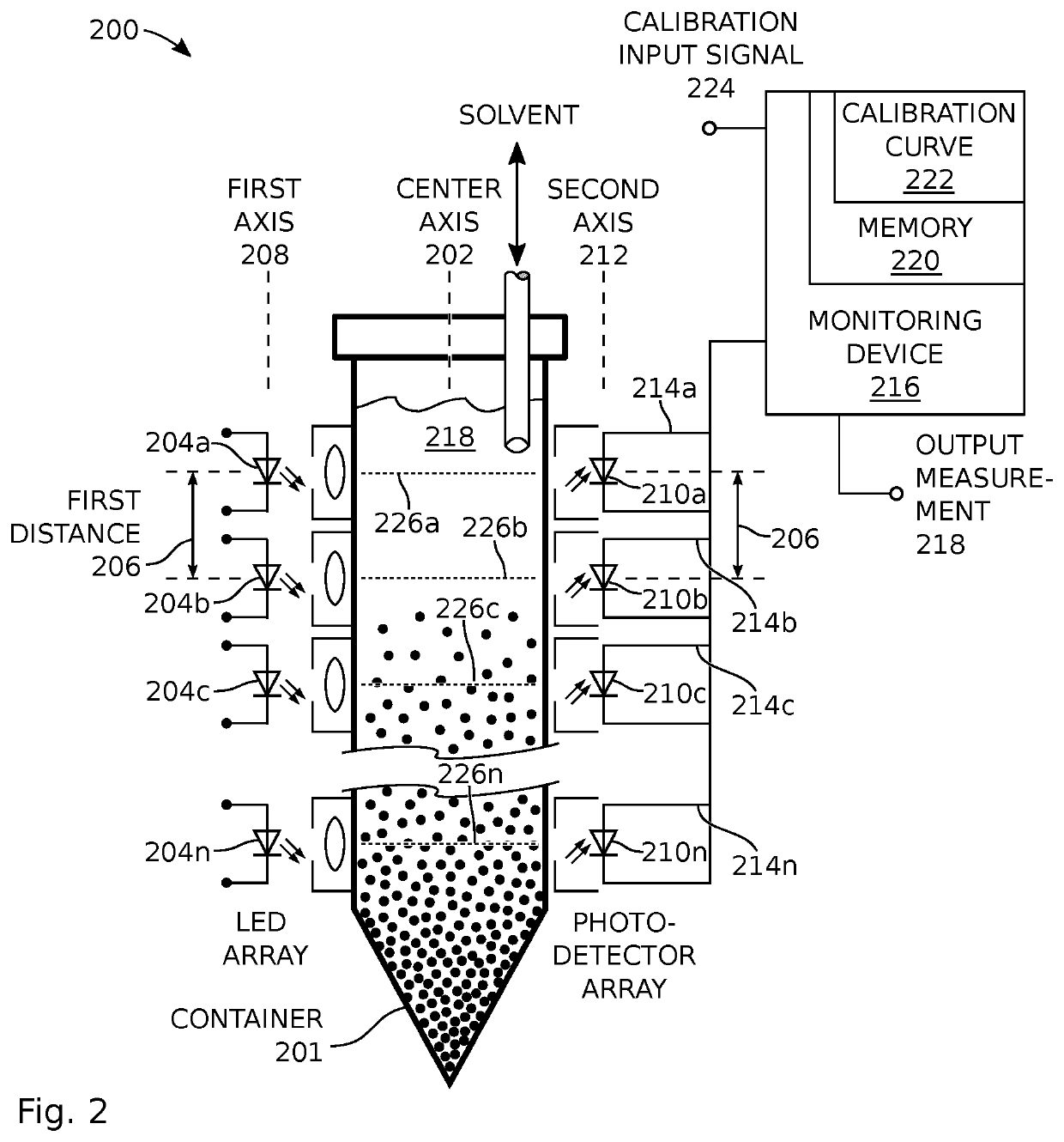
[0054]FIG. 2 is a partial cross-sectional view of a system for characterizing a micro-light emitting diode (microLED) suspension. The system 200 comprises a transparent container 201 having a vertical center axis 202. A plurality of light emitting devices 204a through 204n (LED array) is shown with each light emitting device having a predetermined output light intensity, directed towards the center axis 202 of the container 200 and spaced a first predetermined distance 206 from each other along a vertical first axis 208 parallel to the center axis 202, where (n) is an integer greater than 1. A plurality of light detection devices 210a through 210n (photodetector array) is spaced the first predetermined distance 206 from each other along a vertical second axis 212 parallel to the center axis 202. The light detection devices 210a-210n each have an optical input directed towards a corresponding light emitting device output and an output, respectively on lines 214a through 214n, to prov...
PUM
 Abstract
Description
Claims
Application Information