Display device
a technology of display device and substrate, applied in the field of display device, can solve the problems of easy influence and rather high leakage current, and achieve the effect of suppressing the influence of external light and suppressing the charge up in the substra
- Summary
- Abstract
- Description
- Claims
- Application Information
AI Technical Summary
Benefits of technology
Problems solved by technology
Method used
Image

Examples
embodiment 1
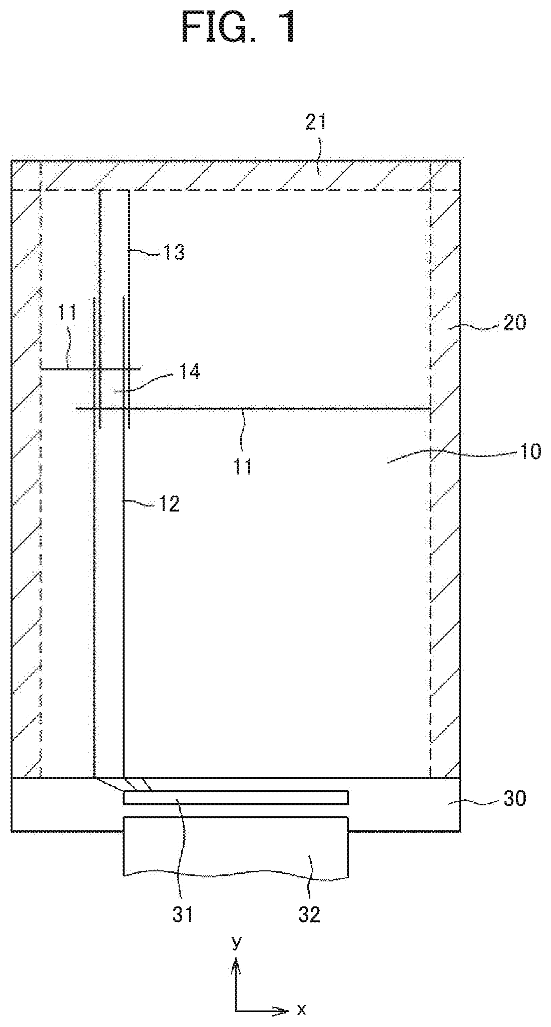
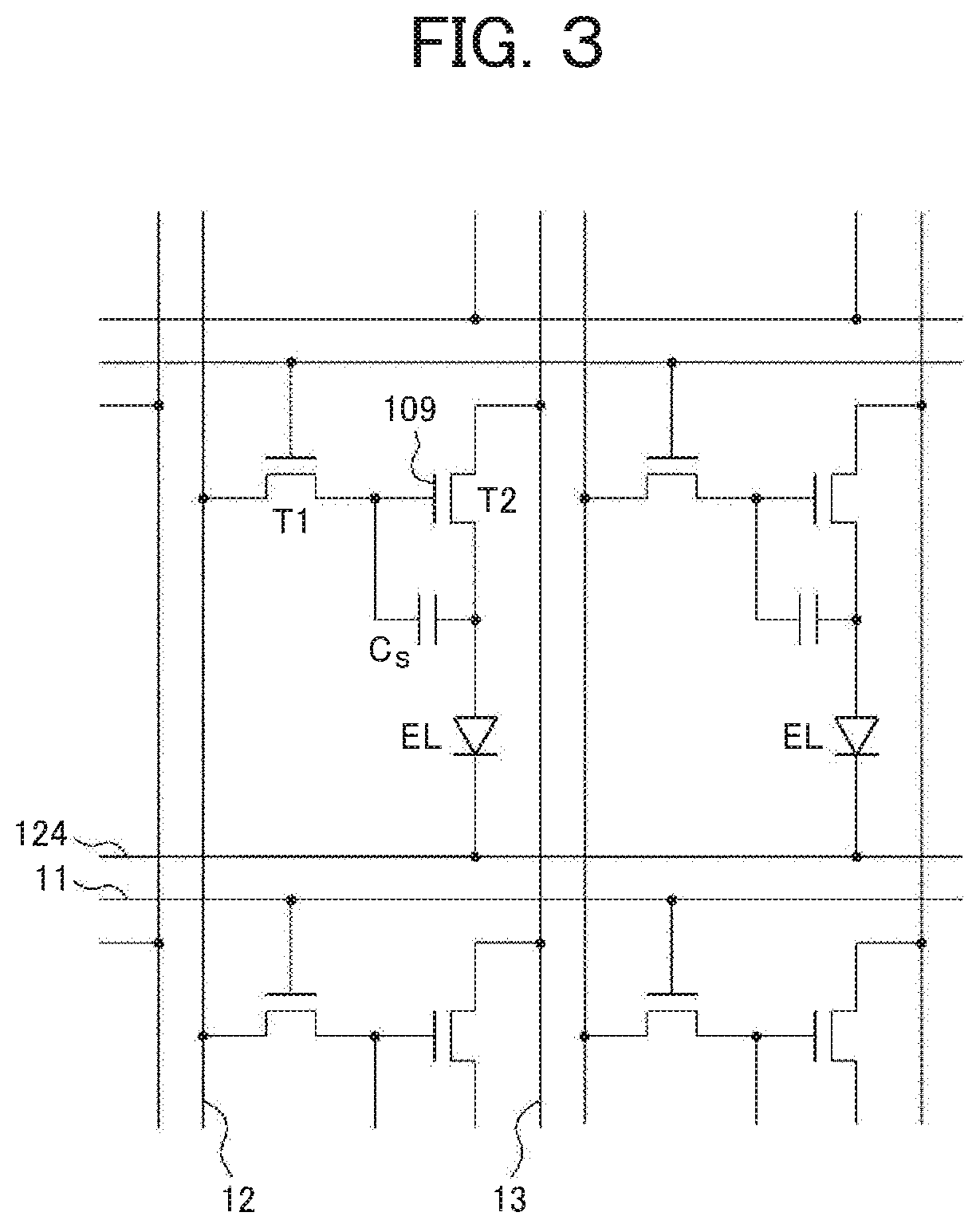
[0045]FIG. 1 is a plan view of the organic EL display device having the flexible substrate 100, which the present invention is applied. The organic EL display device in FIG. 1 has the display area 10 and the terminal area 30. In the display area 10, the scan lines 11 extend in the lateral direction (x direction) and are arranged in the longitudinal direction (y direction). The video signal lines 12 and the power lines 13 extend in the longitudinal direction and are arranged in the lateral direction. The pixel 14 is formed in the area surrounded by the scan lines 11 and the video signal lines 12 or the power lines 33.
[0046]In FIG. 1, the terminal area 30 is formed in the area where the display area 10 is not formed; the driver IC 31 is installed in the terminal area 30. The video signals are arranged in the driver IC 31 and supplied to the display area 10. Further, the flexible wiring substrate 32 is connected to the terminal area 30 to supply powers and signals to the organic EL dis...
embodiment 2
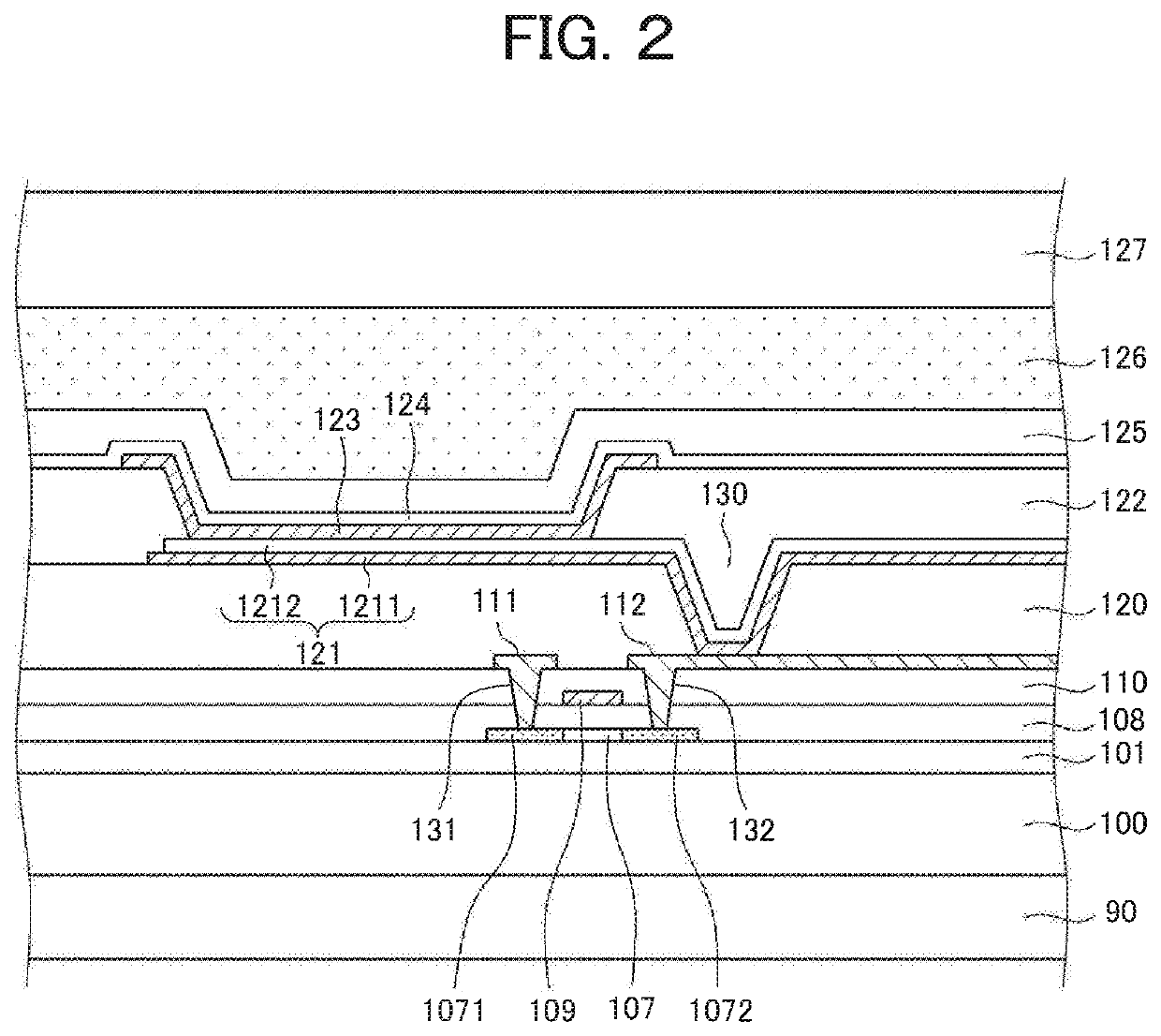
[0095]FIG. 10 is a cross sectional view according to embodiment 2 of the present invention. In embodiment 1, the LIPS film 50 is used for the shield against the charges induced in the TFT substrate 100. In the structure of embodiment 1, there are three insulating films of the second interlayer insulating film 106, the first interlayer insulating film 105 and the first gate insulating film 103 between the oxide semiconductor film 107 and the shield film 50, therefore, increase of the floating capacitance can be suppressed.
[0096]The structure of embodiment 2 shown in FIG. 10 has a shield film 70 formed under the undercoat film 101, thus, the capacitance between the shield film 70 and the oxide semiconductor film 107 can be further decreased. In FIG. 7, the shield film 70 is formed by the conductive material under the undercoat 101. The conductive material is preferably metal, the metal can be the same material as the gate electrode.
[0097]In FIG. 10, there are the second interlayer ins...
embodiment 3
[0105]Embodiment 1 and embodiment 2 explain when the present invention is applied to the organic EL display device. The present invention can be applied to the liquid crystal display device. Namely, flexible display device, using the polyimide substrate, is also required in the liquid crystal display device.
[0106]In the liquid crystal display device, however, unlike the organic EL display device, the driving transistor does not exist in the pixel area, but only the switching transistor exists in the pixel area. However, the switching transistor also is influenced by charge up in the polyimide substrate. Namely, the threshold voltage of the switching transistor is influenced by the charge up of the polyimide substrate, consequently, the charges in the pixel capacitance according to the video signal get influenced.
[0107]FIG. 14 is a plan view of the liquid crystal display device. In FIG. 14, the TFT substrate 100 adheres to the counter substrate 200 through the sealant 40 and the liqu...
PUM
| Property | Measurement | Unit |
|---|---|---|
| thickness | aaaaa | aaaaa |
| temperature | aaaaa | aaaaa |
| thick | aaaaa | aaaaa |
Abstract
Description
Claims
Application Information
 - R&D
- Intellectual Property
- Life Sciences
- Materials
- Tech Scout
- Unparalleled Data Quality
- Higher Quality Content
- 60% Fewer Hallucinations
Browse by: Latest US Patents, China's latest patents, Technical Efficacy Thesaurus, Application Domain, Technology Topic, Popular Technical Reports.
© 2025 PatSnap. All rights reserved.Legal|Privacy policy|Modern Slavery Act Transparency Statement|Sitemap|About US| Contact US: help@patsnap.com