Optoelectronic device comprising a matrix of three-dimensional diodes
- Summary
- Abstract
- Description
- Claims
- Application Information
AI Technical Summary
Benefits of technology
Problems solved by technology
Method used
Image
Examples
first embodiment
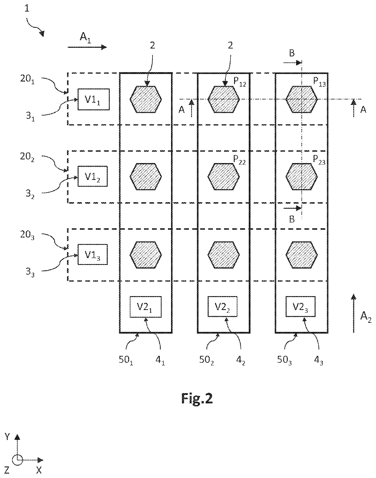
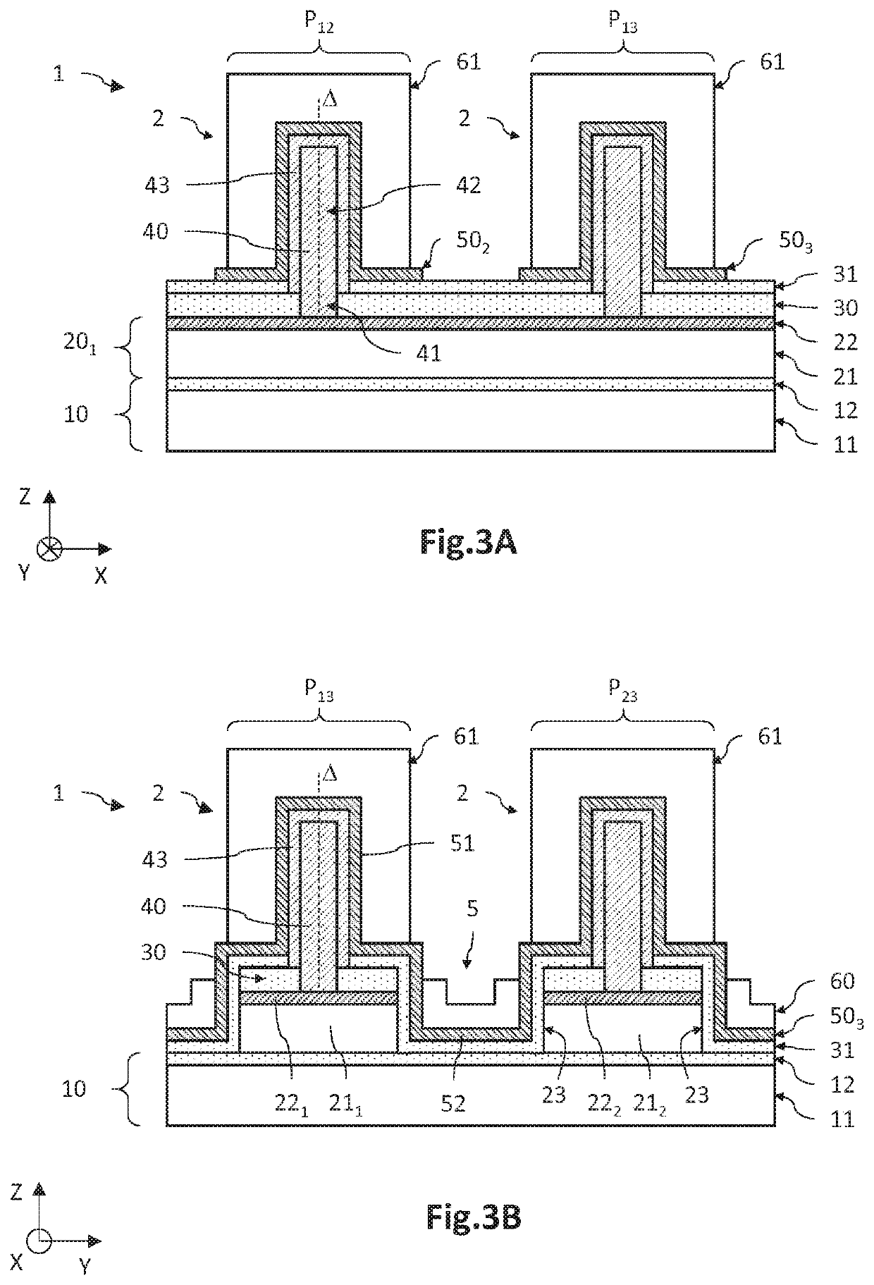
[0035]FIG. 2 and FIGS. 3A and 3B illustrate an optoelectronic device 1 with a matrix of pixels each comprising one or more light-emitting diodes 2. FIG. 2 is a schematic and partial top view, and FIGS. 3A and 3B are schematic and partial sectional views along the plane A-A and B-B, respectively.
[0036]Defined here and for the rest of the description is a three-dimensional direct coordinate system XYZ, where the axes X and Y form a plane parallel to the main plane of the substrate, and where the axis Z is oriented in a manner substantially orthogonal to the front face of the substrate. Furthermore, the terms “lower” and “upper” are understood to relate to positions that are nearer to and further from the front face of the substrate in the +Z direction.
[0037]In general, the optoelectronic device 1 comprises:[0038]a carrier 10;[0039]a plurality of separate first electrodes 20, extending longitudinally parallel to an axis A1, each first electrode 20 being formed of a stack of a longitudi...
second embodiment
[0089]FIGS. 5A and 5B are schematic and partial views, in section along the plane A-A and B-B, respectively, of an optoelectronic device1 according to a
[0090]The optoelectronic device 1 according to the second embodiment differs from that illustrated in FIGS. 3A and 3B, in particular, in that the trench isolations 5 are filled with a dielectric material, so as to form a planar surface together with the upper face of the conductive nucleation strips 22. Thus, the first intermediate insulating layer 30 (growth mask) extends continuously in a planar manner.
[0091]The first electrodes 20 are electrically isolated from the neighbors by trench isolations 5, for example of the STI (for shallow trench isolation) type, which extend along the lateral flanks 23 of the first electrodes 20 down to the lower insulating layer 12.
[0092]The growth mask (first intermediate insulating layer 30) is coated locally with the transparent conductive strips 50. It thus provides the electrical insulation betwe...
third embodiment
[0102]FIGS. 7A and 7B are schematic and partial views, in section along the plane A-A and B-B, of two variants of an optoelectronic device 1 according to a
[0103]The optoelectronic device 1 according to the third embodiment differs from those illustrated in FIGS. 3A and 3B and FIGS. 5A and 5B primarily in that the longitudinal conductive portions 21 are formed inside a semiconductor layer 13 of the carrier 10 from an upper face thereof, and are electrically insulated from one another via reverse-biased p-n junctions (depletion). In other words, each longitudinal conductive portion 21 is formed of a longitudinal well, i.e., of a region doped according to the first conductivity type (identical to that of the first doped portions 40 of the diodes 2) of the semiconductor layer 13 doped according to the second conductivity type.
[0104]By way of example, with reference to FIG. 7A, the carrier 10 is formed here of a stack of a thick layer 11, of a lower insulating layer 12 and of a semicondu...
PUM
 Abstract
Description
Claims
Application Information


