Non-volatile memory device and method of writing to non-volatile memory device
a non-volatile memory and memory device technology, applied in the direction of digital storage, electric digital data processing, instruments, etc., can solve the problem of rapid growth of concerns, and achieve the effect of reducing correlation
- Summary
- Abstract
- Description
- Claims
- Application Information
AI Technical Summary
Benefits of technology
Problems solved by technology
Method used
Image

Examples
embodiment
[0066][Outline of Variable Resistance Non-Volatile Memory Device Used in the Present Disclosure]
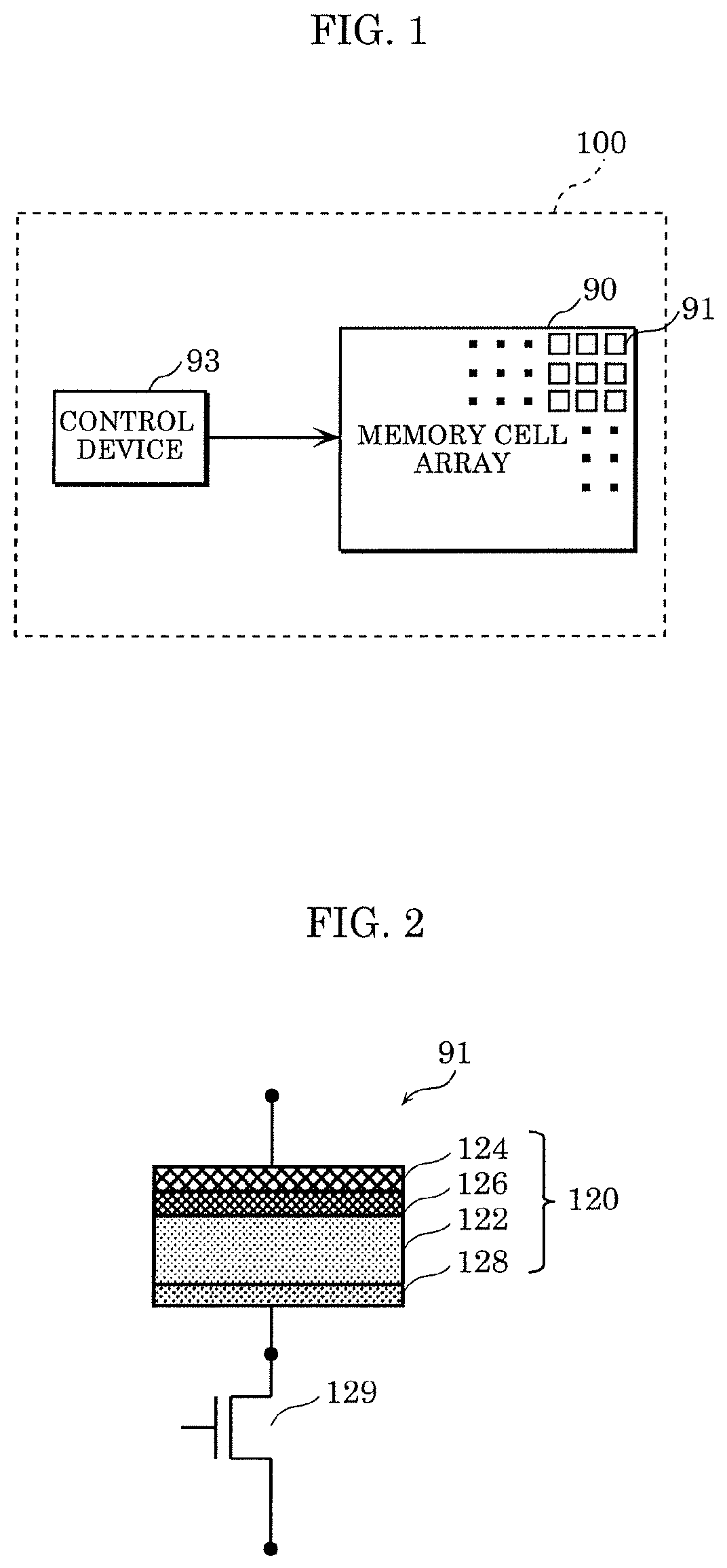
[0067]FIG. 1 is a block diagram of an example of a schematic configuration of variable resistance non-volatile memory device 100 according to an embodiment. FIG. 2 is a cross-sectional view of an example of a schematic configuration of memory cell 91 included in variable resistance non-volatile memory device 100 according to the embodiment. In the following description, a variable resistance non-volatile memory device is also referred to simply as a non-volatile memory device.
[0068]In the example illustrated in FIG. 1, non-volatile memory device 100 according to the present embodiment includes at least memory cell array 90 and control device 93. Control device 93 does not always have to be part of non-volatile memory device 100, and the operation described below may be performed using a control device externally connected to non-volatile memory device 100.
[0069]Memory cell array 90 includ...
example 1
[0108]FIG. 9 illustrates data patterns of memory groups generated by an operation of non-volatile memory device 10 according to Example 1. Each of the memory groups includes at least one data cell and at least one dummy cell which are associated with each other. Data cells are memory cells included in information area 7, and dummy cells are memory cells included in dummy area 8. FIG. 9 illustrates memory groups respectively corresponding to word lines WL0 to WL3. In the present example, k=16, the number of sense amplifier circuits 30 is sixteen, the number of data cells is eight, and the number of dummy cells is eight. For example, focusing on word line WL0, the memory group corresponding to word line WL0 includes sixteen memory cells a to p. Specifically, memory cells a to h are data cells included in information area 7, and memory cells i to p are dummy cells included in dummy area 8. Read operations are performed on memory cells a to p in parallel, and write operations are perfor...
example 2
[0116]Since Example 2 relates to PUF data, a general PUF operation system will be described first, and then an example of an operation of non-volatile memory device 10 according to Example 2 will be described.
[0117]First, the flow of PUF data registration will be described with reference to FIG. 11 and FIG. 12.
[0118]FIG. 11 is a flowchart of an operation example of non-volatile memory device 10 at the time of PUF data registration according to Example 2. FIG. 12 illustrates an operation of non-volatile memory device 10 at the time of PUF data registration according to Example 2.
[0119]In step S21, for example, variations in resistance value of the memory cells in the PUF area set to the low resistance state are detected, and PUF data (P) with n-bits is generated. In step S22, random number data (R) is generated separately from the PUF data. In step S23, code data (C) having a bit length of n bits, which is the combination of the generated random number data (R) and parity data (E) th...
PUM
 Abstract
Description
Claims
Application Information
 - R&D
- Intellectual Property
- Life Sciences
- Materials
- Tech Scout
- Unparalleled Data Quality
- Higher Quality Content
- 60% Fewer Hallucinations
Browse by: Latest US Patents, China's latest patents, Technical Efficacy Thesaurus, Application Domain, Technology Topic, Popular Technical Reports.
© 2025 PatSnap. All rights reserved.Legal|Privacy policy|Modern Slavery Act Transparency Statement|Sitemap|About US| Contact US: help@patsnap.com