Multi-junction solar cell

a solar cell and multi-junction technology, applied in the direction of basic electric elements, electrical apparatus, semiconductor devices, etc., can solve the problems of reducing the efficiency of the solar cell as a whole, higher series resistive losses in the multi-junction solar cell, and greater shadowing, so as to improve the transverse conduction effect, improve the efficiency of the solar cell, and improve the effect of transverse conduction

Pending Publication Date: 2020-12-17
AZUR SPACE SOLAR POWER
View PDF3 Cites 0 Cited by
  • Summary
  • Abstract
  • Description
  • Claims
  • Application Information

AI Technical Summary

Benefits of technology

[0046]A superlattice layer made of alternating InGaP and InAlP layers can have a significantly higher conductivity than an AlInGaP bulk layer of equal thickness due to the better transverse conduction in the InGaP wells.
[0047]In comparison with an exclusively AlInGaP cell, slight voltage losses do still arise. But the voltage losses are smaller in comparison with the losses of an exclusively InGaP cell, and the efficiency of the solar cell with a superlattice structure in the emitter is increased as a result, since the improvements due to the reduced sheet resistance predominate substantially.

Problems solved by technology

The higher sheet resistance of the InAlGaP upper cell results in higher series resistive losses in the multi-junction solar cell, in particular at higher currents.
However, this results in greater shadowing, reducing the efficiency of the solar cell as a whole.
However, in this design a substantial voltage loss of approximately 160 mV nevertheless occurs as compared with an exclusively InAlGaP cell.

Method used


Image

  • Multi-junction solar cell

Examples


Embodiment Construction

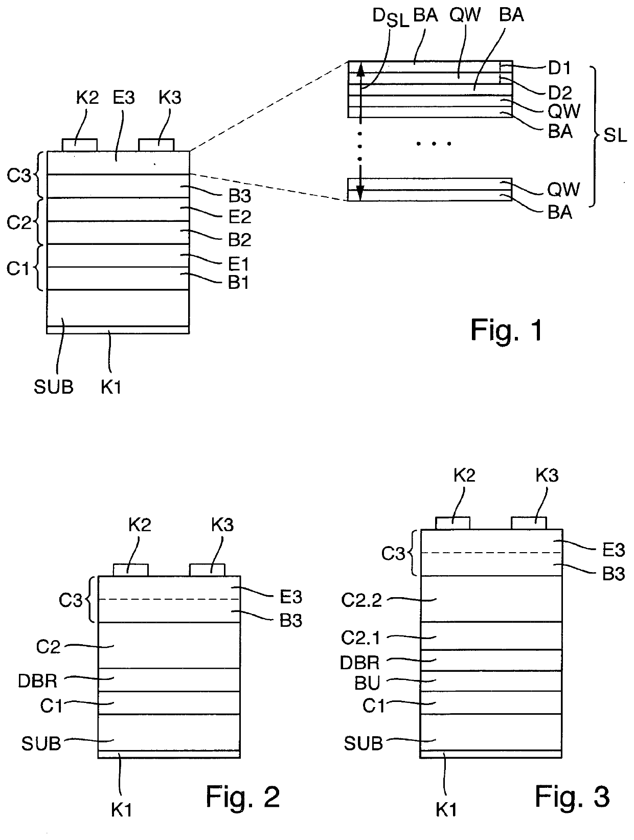
[0059]The illustration in FIG. 1 shows a view of an exemplary embodiment of a stacked multi-junction solar cell MJ, comprising a stack ST composed of a substrate layer SUB, a bottom subcell C1, a middle subcell C2, and a top subcell C3. A full-area contact layer K1 is formed on an underside of the stack ST. Contact fingers K2, K3 are arranged on a top surface of the stack.

[0060]Each subcell C1, C2, and C3 has one base B1, B2, B3 and one emitter E1, E2, E3 each, wherein emitter E3 and base B3 of the top subcell C3 are each made of a III-V semiconductor material.

[0061]The emitter E3 of the top subcell C3 includes a superlattice SL. The superlattice includes multiple thin well layers QW with the thickness D2 and multiple thin barrier layers BA with the thickness D1, wherein the well layers QW and the barrier layers BA are stacked on one another in alternation. The total thickness of the superlattice DSL results from the thickness of the alternating layers and the number of periods.

[006...


PUM

PropertyMeasurementUnit
thicknessaaaaaaaaaa
thicknessaaaaaaaaaa
thicknessaaaaaaaaaa

Abstract

A stacked multi-junction solar cell comprising a stack composed of a bottom subcell, at least one middle subcell, and a top subcell, wherein each subcell has an emitter and a base at least the top subcell is made of a III-V semiconductor material or includes a III-V semiconductor material, and the emitter of the top subcell includes a superlattice.

Description

[0001]This nonprovisional application is a continuation of International Application No. PCT / EP2019 / 000057, which was filed on Feb. 26, 2019, and which claims priority to German Patent Application No. 10 2018 001 592.1, which was filed in Germany on Mar. 1, 2018, and which are both herein incorporated by reference.BACKGROUND OF THE INVENTIONField of the Invention[0002]The present invention relates to a multi-junction solar cell.Description of the Background Art[0003]In order to better utilize the solar spectrum, multi-junction solar cells generally comprise three or more subcells with different band gaps that are matched to one another, wherein the top subcell has the largest band gap and the bottom subcell has the smallest band gap, and the top subcell is located on the sun-facing side of the multi-junction solar cell.[0004]Such multi-junction solar cells are known, for example from the paper “Development of Upright Metamorphic 4J Space Solar Cells,” by W. Guter et al., Space Power...

Claims


Application Information

Patent Timeline
Patent Type & Authority Applications(United States)
IPC IPC(8): H01L31/0687H01L31/0352H01L31/0304
CPCH01L31/0687H01L31/035236H01L31/03046Y02E10/544
Inventor FUHRMANN, DANIELKELLER, GREGORVAN LEEST, ROSALINDA
Owner AZUR SPACE SOLAR POWER
Why Eureka
Try Eureka