Methods of forming silicon germanium structures

a technology of silicon germanium and structure, applied in the direction of semiconductor devices, electrical devices, nanotechnology, etc., can solve the problems of relatively undetected large interface layers with subsequently grown si layers, and low growth rate of silicon layers at such temperatures, and achieve faster growth rates of layers. , the effect of high temperatur

Active Publication Date: 2021-01-21
ASM IP HLDG BV
View PDF5 Cites 154 Cited by
  • Summary
  • Abstract
  • Description
  • Claims
  • Application Information

AI Technical Summary

Benefits of technology

[0011]Various embodiments of the present disclosure provide improved methods for forming structures including layers comprising SiGe (SiGe layers). While the ways in which the various drawbacks of the prior art are discussed in greater detail below, in general, exemplary methods include

Problems solved by technology

Unfortunately, Ge on the surface of the SiGe layer is energetically more favorable than Si on the surface.
SiGe layers can be grown using dichlorosilane (DCS) at temperatures between about 600° C. and 700° C. Such techniques result in relatively low growth rates of the SiGe

Method used


Image

  • Methods of forming silicon germanium structures
  • Methods of forming silicon germanium structures
  • Methods of forming silicon germanium structures

Examples


Embodiment Construction

[0022]Although certain embodiments and examples are disclosed below, it will be understood by those in the art that the invention extends beyond the specifically disclosed embodiments and / or uses of the invention and obvious modifications and equivalents thereof. Thus, it is intended that the scope of the invention disclosed should not be limited by the particular disclosed embodiments described below.

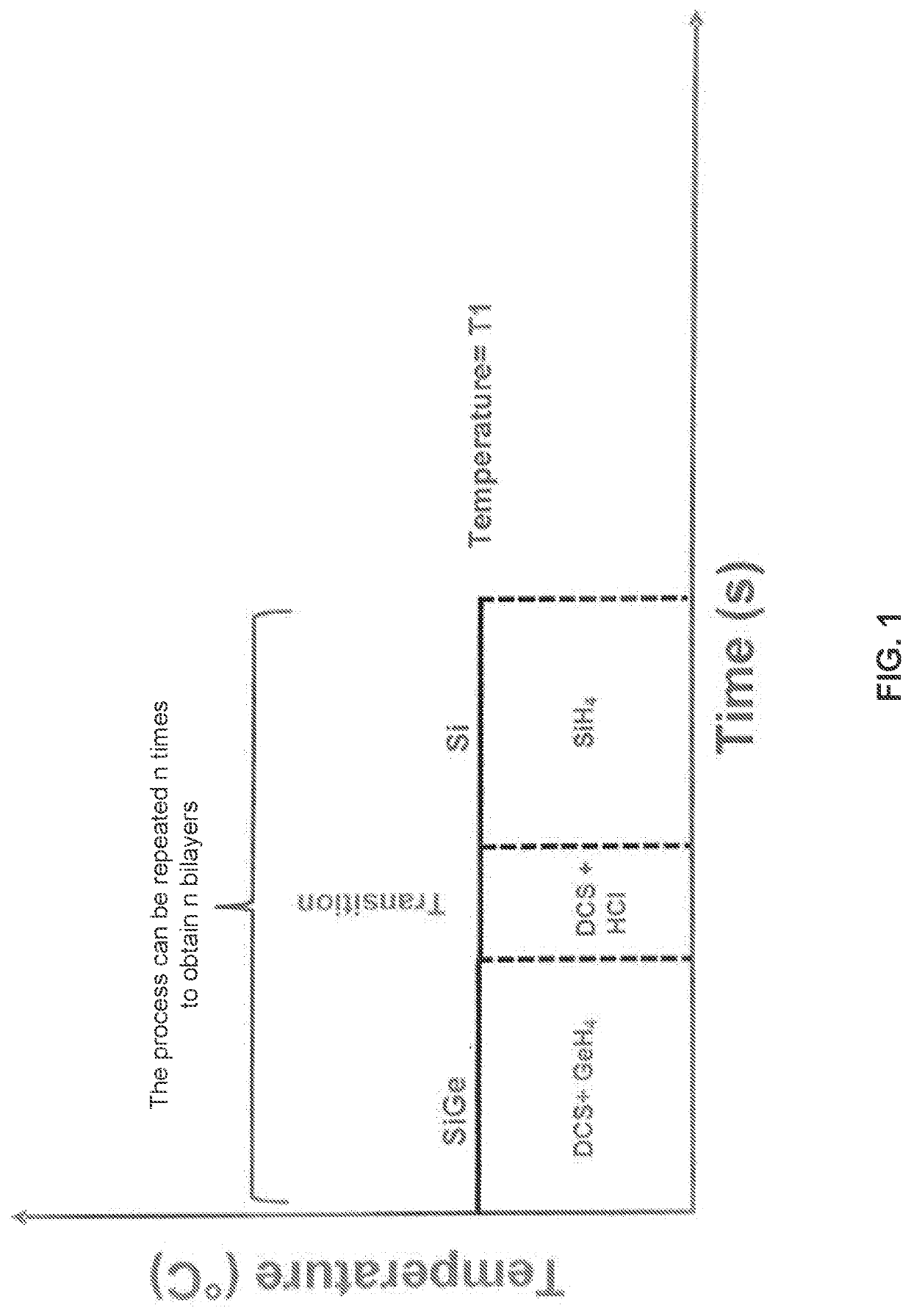
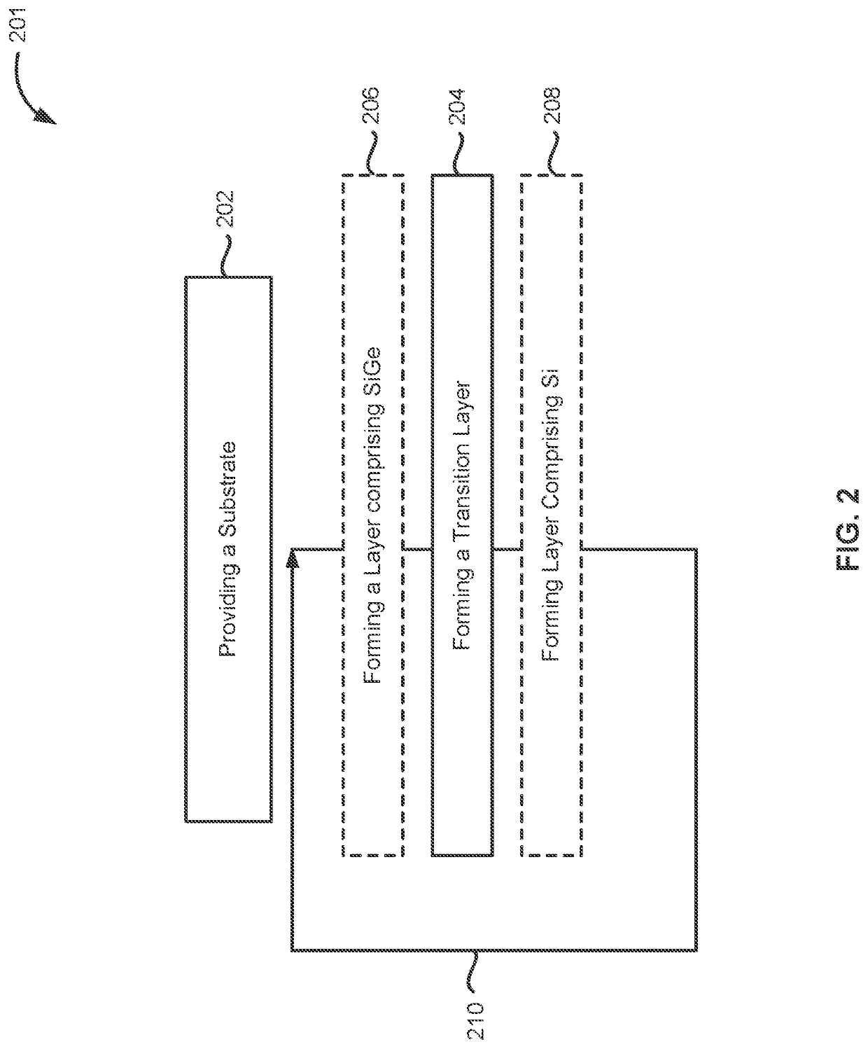
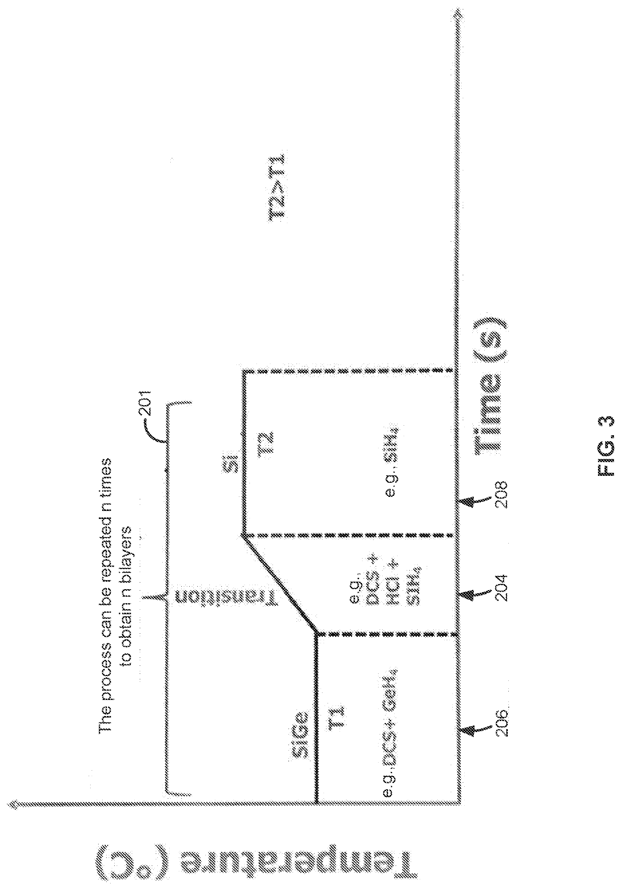
[0023]The present disclosure generally relates to methods of forming structures that include a layer comprising silicon germanium (SiGe) and to structures formed using the methods. Exemplary methods described herein can be used to form structures that include a layer comprising SiGe and a layer comprising silicon (Si) epitaxially formed overlying the layer comprising SiGe, such that an interface layer between the layer comprising SiGe and the layer comprising Si can be relatively small, and such that a transition between the layer comprising SiGe and the layer comprising Si is abrupt. ...


PUM


Abstract

Methods for forming structures that include a layer comprising silicon germanium are disclosed. Exemplary embodiments of the disclosure provide improved methods of forming a transition layer on the layer comprising silicon germanium that can mitigate any formation of an interface layer between the layer comprising silicon germanium and a subsequently formed layer comprising silicon.

Description

CROSS-REFERENCE TO RELATED APPLICATIONS[0001]This application claims priority to U.S. Provisional Patent Application Ser. No. 62 / 875,489 filed Jul. 17, 2019 titled METHODS OF FORMING SILICON GERMANIUM STRUCTURES, the disclosures of which are hereby incorporated by reference in their entirety.FIELD OF DISCLOSURE[0002]The present disclosure generally relates to structures including silicon germanium layers and to methods of forming the structures. More particularly, the disclosure relates to methods of forming a transition and / or passivation layer on SiGe layers and to related structures.BACKGROUND OF THE DISCLOSURE[0003]Because of its relatively low bandgap and potentially relatively high carrier mobility, silicon germanium (SiGe) has been used in the manufacture of various electronic devices, such as photodetectors, thermoelectric devices, bipolar transistors, and field effect transistors, such as metal oxide field effect transistors (MOSFETS).[0004]Recently, in efforts to form devi...

Claims


Application Information

Patent Timeline
IPC IPC(8): H01L21/02H01L29/165
CPCH01L21/0262H01L29/165H01L21/02532H01L21/0245H01L21/02381B82Y10/00H01L29/66439H01L29/0673H01L29/161H01L21/0251H01L29/42392
Inventor KHAZAKA, RAMIBARBOSA LIMA, LUCAS PETERSEN
Owner ASM IP HLDG BV
Why Eureka
Try Eureka