Unlock instant, AI-driven research and patent intelligence for your innovation.

Semiconductor device

Active Publication Date: 2021-01-21
LG INNOTEK CO LTD
View PDF0 Cites 1 Cited by
  • Summary
  • Abstract
  • Description
  • Claims
  • Application Information

AI Technical Summary

Benefits of technology

The patent describes a way to make a semiconductor device that has better performance at low current levels. It also helps to increase the output power of the device's optical output. The advantages of this invention include improved performance at low current levels and increased optical output power.

Problems solved by technology

However, there is a problem in that reduced optical output power is provided when current density decreases as the size of the light-emitting device decreases.

Method used


Image

  • Semiconductor device
  • Semiconductor device
  • Semiconductor device

Examples


Embodiment Construction

[0036]While the present invention is susceptible to various modifications and alternative forms, particular exemplary embodiments thereof are shown by way of example in the drawings and will herein be described in detail. It should be understood, however, that there is no intent to limit the present invention to the particular forms disclosed, but on the contrary, the present invention is to cover particular modifications, equivalents, and alternatives falling within the spirit and scope of the present invention.

[0037]It will be understood that, although the terms “first,”“second,” and the like may be used herein to describe various elements, these elements should not be limited by these terms. These terms are only used to distinguish one element from another. For example, a first element could be termed a second element, and a second element could similarly be termed a first element without departing from the scope of the present invention. As used herein, the term “and / or” include...


PUM


Abstract

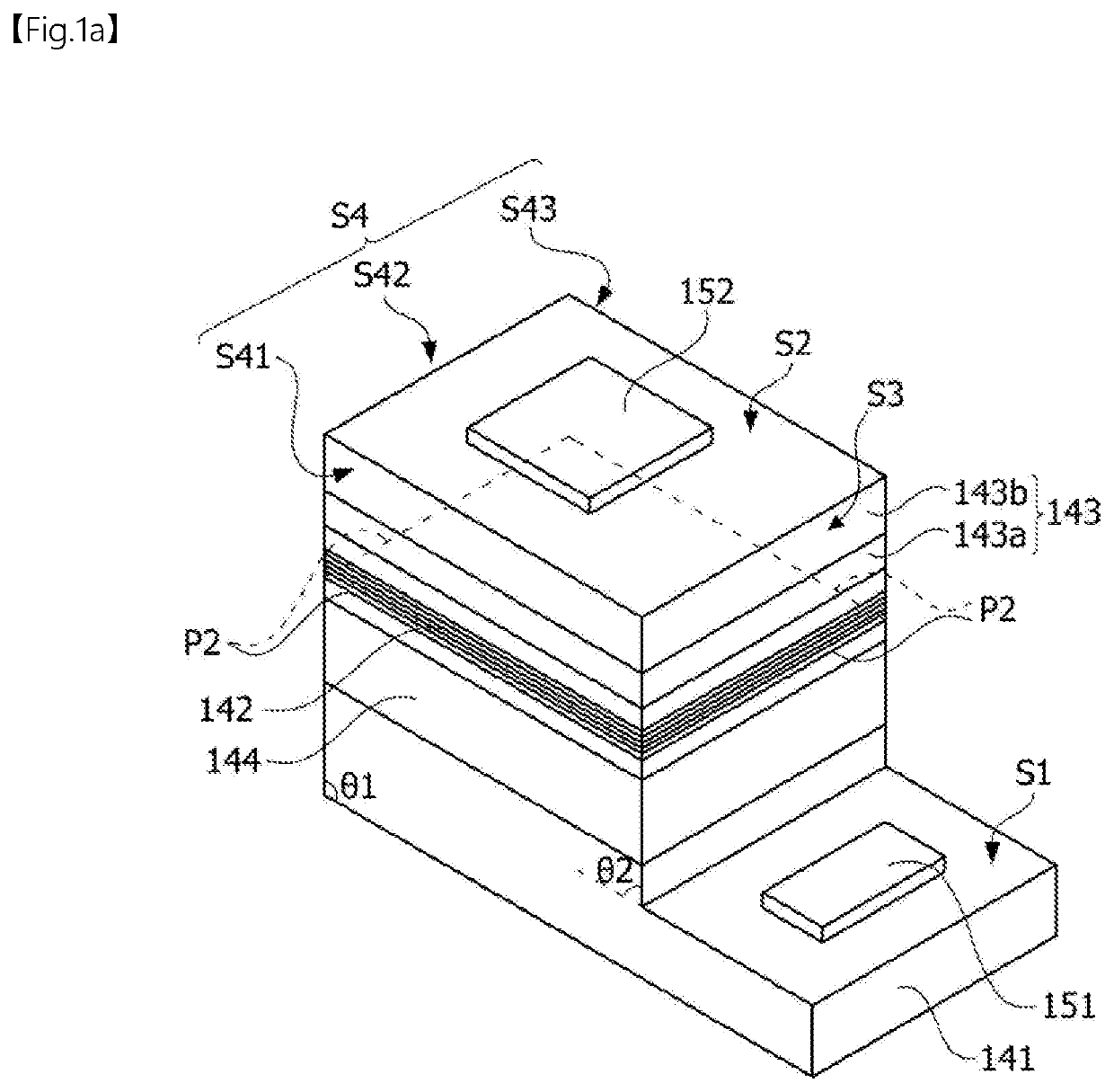
In an embodiment, disclosed is a semiconductor device comprising: a semiconductor structure which comprises a first conductive semiconductor layer, a second conductive semiconductor layer, and an active layer disposed between the first conductive semiconductor layer and the second conductive semiconductor layer; a first electrode which is electrically connected to the first conductive semiconductor layer; and a second electrode which is electrically connected to the second conductive semiconductor layer, wherein an area ratio between an area of an upper surface of the second conductive semiconductor layer and an area of an outer surface of the active layer is 1:0.0005 to 1:0.01.

Description

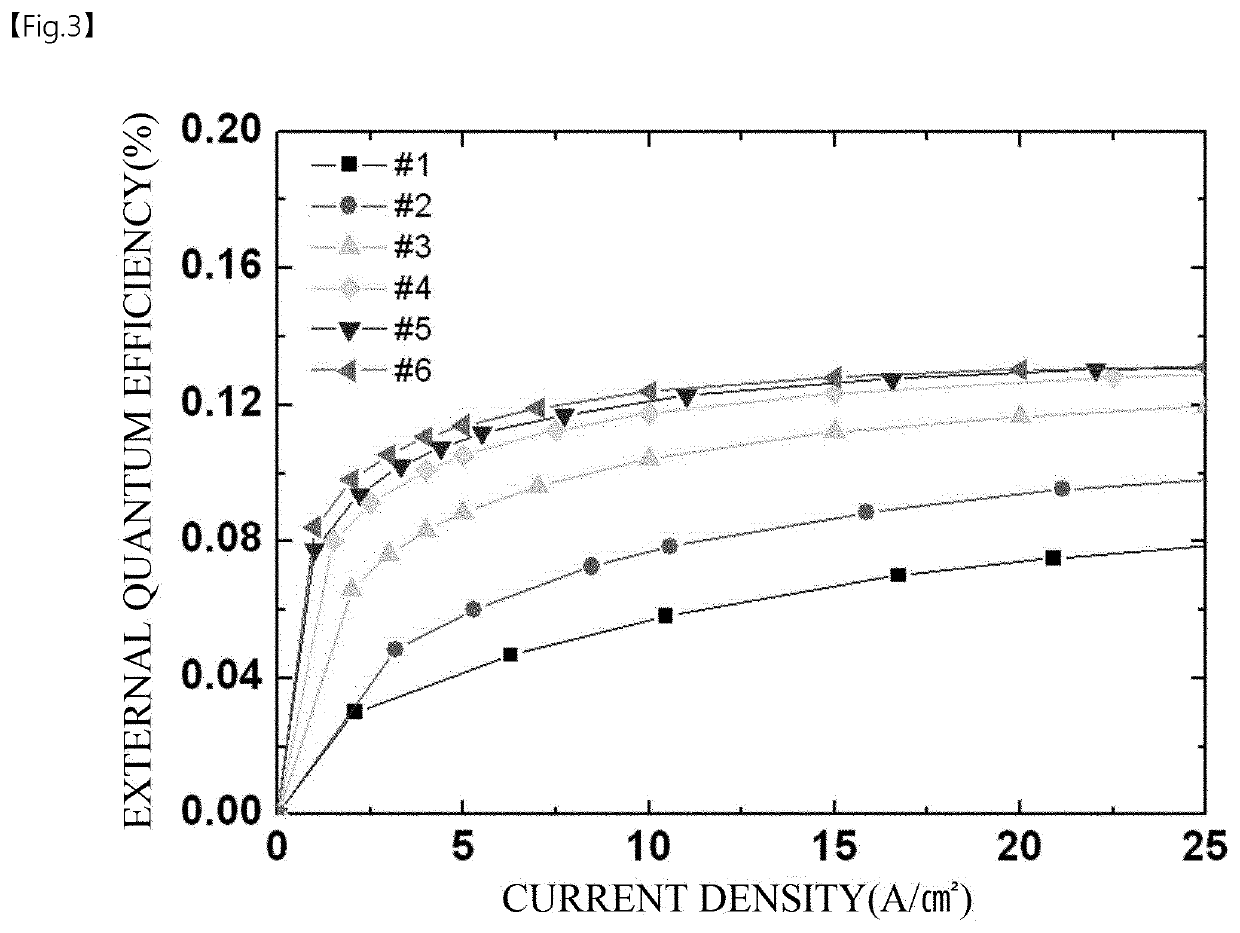
TECHNICAL FIELD[0001]Embodiments relate to a semiconductor device.BACKGROUND ART[0002]A light-emitting diode (LED) is one of light-emitting devices that emit light when current is applied. The LED may emit high-efficiency light at a low voltage and thus has an excellent energy saving effect. Recently, since the luminance problem of the LED has been significantly improved, LEDs are being applied to various devices such as backlight units of liquid crystal display devices, electric signboards, indicators, and home appliances.[0003]Further, studies for reducing the size of a light-emitting device are actively being conducted in various fields. For example, in a display field, resolution may be improved as the size of the light-emitting device decreases.[0004]However, there is a problem in that reduced optical output power is provided when current density decreases as the size of the light-emitting device decreases.DISCLOSURETechnical Problem[0005]An embodiment is directed to providing ...

Claims


Application Information

Patent Timeline
IPC IPC(8): H01L33/38H01L33/30
CPCH01L33/382H01L33/30H01S5/00H01L33/20H01L33/06H01L33/36H01L33/32
Inventor MOON, YONG TAEMOON, JI HYUNGLEE, SANG YOUL
Owner LG INNOTEK CO LTD
Features
  • R&D
  • Intellectual Property
  • Life Sciences
  • Materials
  • Tech Scout
  • Unparalleled Data Quality
  • Higher Quality Content
  • 60% Fewer Hallucinations
Learn More