Inductor component

Pending Publication Date: 2021-01-28
MURATA MFG CO LTD
View PDF4 Cites 0 Cited by
  • Summary
  • Abstract
  • Description
  • Claims
  • Application Information

AI Technical Summary

Benefits of technology

[0007]Accordingly, the present disclosure provides an inductor component wherei

Problems solved by technology

When the inductor component contains the glass-based insulating material, the strength of the inductor component may be reduced, and cracking may occur in the element assembly of the inductor component due to impact during mounting and stress during substrate bending.
Addition of the crystalline filler enhances the strength of the glass-based insulating material on the one hand but causes a new problem that the Q-value is not sufficiently increased on the other hand.
For example, since the permittivity

Method used


Image

  • Inductor component
  • Inductor component
  • Inductor component

Examples


Example

First Embodiment

[0054]Configuration

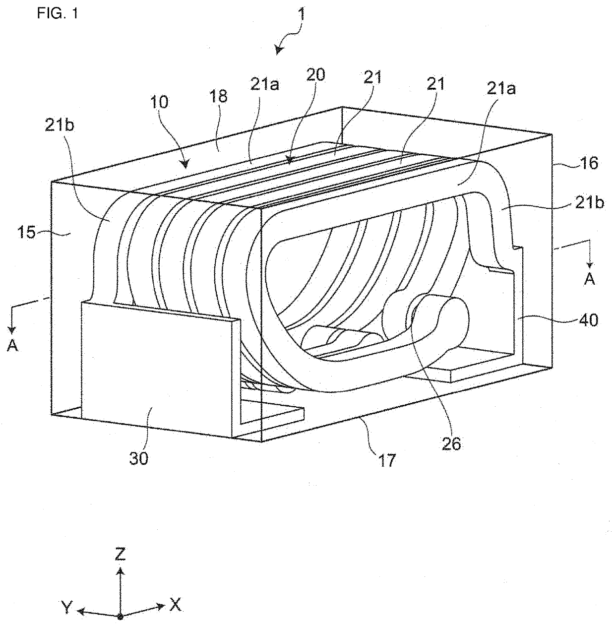
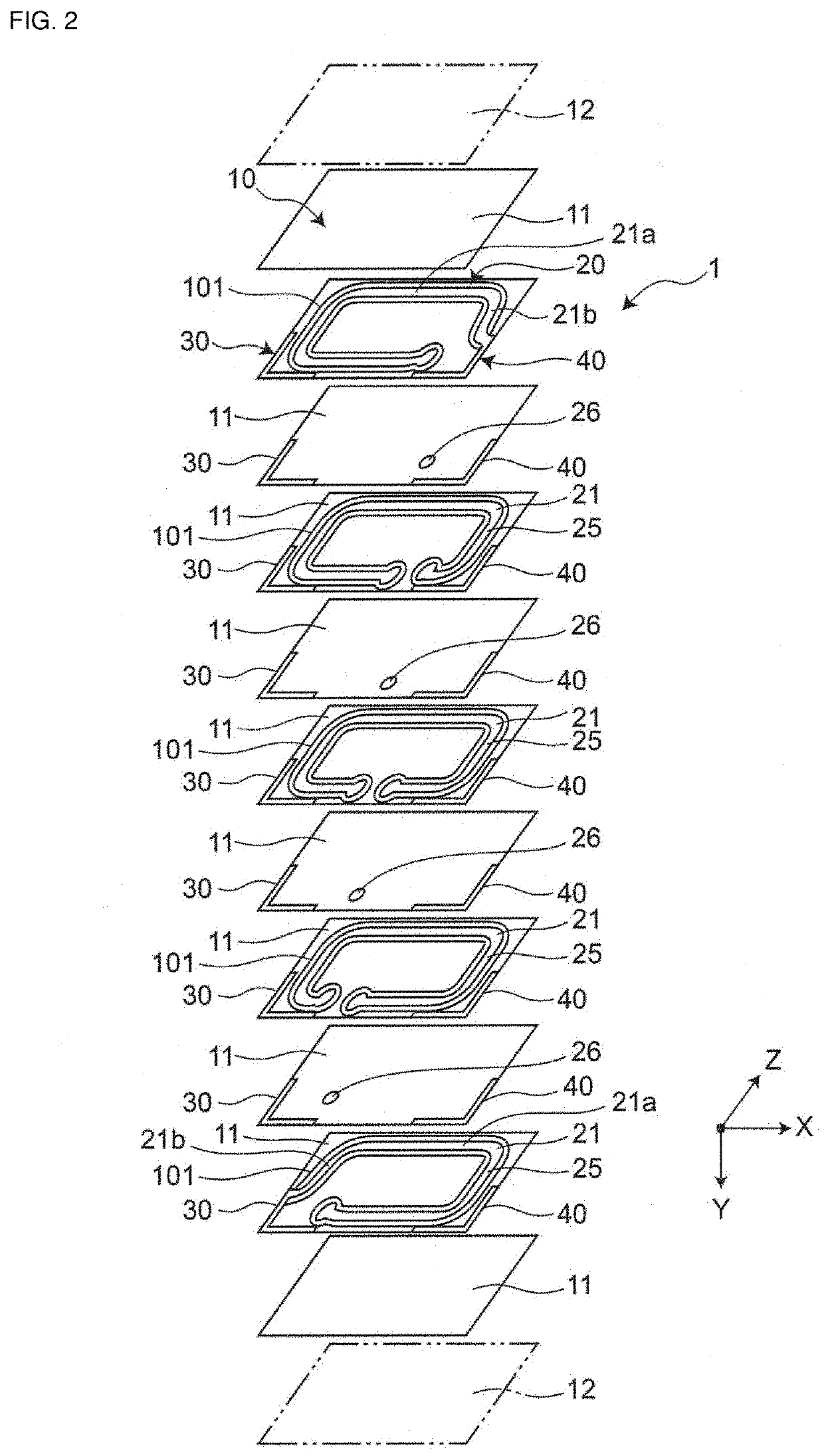
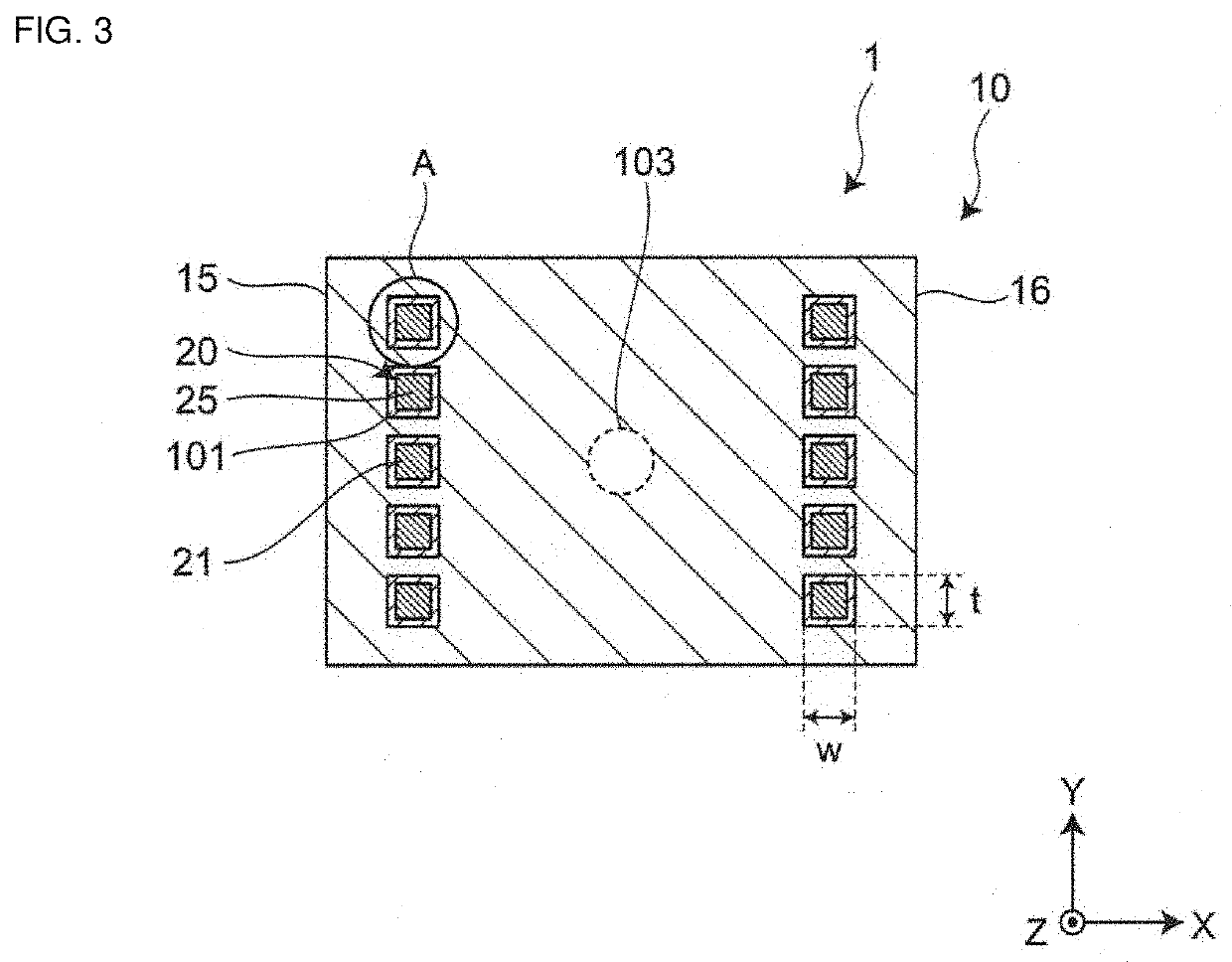
[0055]FIG. 1 is a perspective view showing a first embodiment of an inductor component. FIG. 2 is an exploded perspective view showing the first embodiment of the inductor component. FIG. 3 is a sectional view cut along line A-A in FIG. 1. FIG. 4 is a magnified partial view of the diagram (diagram showing a magnified portion A) in FIG. 3.

[0056]As shown in FIG. 1 and FIG. 2, the inductor component 1 includes an element assembly 10, a coil 20 that is an inner electrode arranged in the element assembly 10, and a first outer electrode 30 and a second outer electrode 40 that are electrically coupled to the coil 20. In FIG. 1, the element assembly 10 is expressed as being transparent so that the internal structure (in particular, the structure of the coil 20) of the element assembly 10 is readily understood. Meanwhile, in FIG. 1, a filler-poor glass portion is omitted so that the internal structure of the element assembly 10 is readily understood.

[0057]T...

Example

Example

[0120]The inductor component 1 of the example had a structure in which the insulating layers 11 provided with the coil conductor layer 25 were directly stacked.

[0121]Mother Multilayer Body Formation Step

[0122]An insulating paste layer was formed by repeating application of an insulating paste containing the borosilicate glass as a primary component by screen printing. The insulating paste layer was an outer-layer insulating layer located outside the coil conductor layer 25 in the stacking direction. The borosilicate glass contained B, Si, O, and K.

[0123]The photosensitive conductor paste layer was formed on the outer-layer insulating layer by coating. The coil conductor layer 25 and the outer conductor layer were formed by a photolithography step. Specifically, the photosensitive conductor paste layer was formed by applying the photosensitive conductor paste containing Ag as a metal primary component by screen printing. The photosensitive conductor paste layer was irradiated ...

Example

Second Embodiment

[0138]FIG. 8 is a sectional view showing a second embodiment of an inductor component 1A. The second embodiment is different from the first embodiment in that the thickness of the filler-poor glass portion 101 near to the outer edge of the coil conductor layer 25 is different from the thickness near to the inner edge of the coil conductor layer 25. The configuration including this difference will be described below. In the second embodiment, the same references as in the first embodiment indicate the same configurations as in the first embodiment and explanations thereof are omitted.

[0139]As shown in FIG. 8, the inductor component 1A according to the second embodiment includes a first filler-poor glass portion 101A and a second filler-poor glass portion 101B. In a plane perpendicular to the winding axis of the coil 20, the first filler-poor glass portion 101A is in contact with the outer edge of the coil wiring line 21, and the second filler-poor glass portion 101B ...


PUM

PropertyMeasurementUnit
Fractionaaaaaaaaaa
Thicknessaaaaaaaaaa
Contentaaaaaaaaaa

Abstract

An inductor component includes an element assembly formed of an insulator material and an inner electrode arranged in the element assembly. The insulator material contains a base material formed of an amorphous material containing B, Si, O, and K and a crystalline filler and includes a filler-poor glass portion in a region along the inner electrode. The content of the crystalline filler in the filler-poor glass portion is lower than the content of the crystalline filler in the element assembly excluding the filler-poor glass portion.

Description

CROSS-REFERENCE TO RELATED APPLICATION[0001]This application claims benefit of priority to Japanese Patent Application No. 2019-136881, filed Jul. 25, 2019, the entire content of which is incorporated herein by reference.BACKGROUNDTechnical Field[0002]The present disclosure relates to an inductor component.Background Art[0003]In recent years, in accordance with higher frequencies of communication equipment, for example, cellular phones, many surface-mounting type small multilayer coils (hereafter referred to as inductor components) compatible with high frequencies in a GHz band have been adopted in sending portions and receiving portions of the communication equipment. In particular, regarding the inductor components, to address high frequencies, it is desirable that insulating portions exhibit low permittivity and low dielectric loss and it is desirable that conductor portions exhibit low resistance and low loss. To satisfy such demands, the materials and the shapes of the inductor...

Claims


Application Information

Patent Timeline
IPC IPC(8): H01F27/32C03B19/06C03C10/00H01F17/00
CPCH01F27/323C03B19/06H01F2017/004H01F17/0013C03C2214/20C03C10/0054H01F27/2804H01F27/324H01F27/34H01F2027/2809H01F27/292C03C8/16C03C8/18C03C17/3411
Inventor SANO, RIKIYAKONDO, KENTAOOTA, YOSHIYUKI
Owner MURATA MFG CO LTD
Why Eureka
Try Eureka