
Organic light emitting diode display panel and manufacturing method thereof, and display device

a technology of light-emitting diodes and display panels, which is applied in the field of display technologies, can solve the problems of affecting the life of the oled, the rapid decay of the device, and the possibility of a larger package failure, so as to improve the water-oxygen barrier property of the hydrophobic film layer, improve the water-oxygen barrier ability of the hydrophobic membrane layer, and reduce the direct contact between the water and the hydrophobic film layer

Active Publication Date: 2021-02-04
WUHAN CHINA STAR OPTOELECTRONICS SEMICON DISPLAY TECH CO LTD
View PDF0 Cites 0 Cited by
  • Summary
  • Abstract
  • Description
  • Claims
  • Application Information

AI Technical Summary

Benefits of technology

The present invention describes a method for improving the water and oxygen barrier properties of a thin film encapsulation layer in a display panel. This is achieved by forming a super-hydrophobic outer layer with a nanometer-scale ultra-thin air layer that reduces direct contact between water and the layer, and a hydrophobic group that improves the contact angle with external liquid. The result is an improved water-oxygen barrier property, reduced penetration of water and oxygen, improved water-blocking ability, and extended lifetime of the display panel.

Problems solved by technology

However, organic light emitting diode (OLED) materials are very sensitive to water and oxygen, and a small amount intrusion of water and oxygen will cause rapid decay of the device, affecting lifetime of the OLED.
However, the thinner the TFE structure, the greater the possibility of package failure under the same conditions, so it is required to develop an encapsulation layer with better water-blocking oxygen resistance.
There is a problem that the encapsulation layer ineffective in the prior art.

Method used

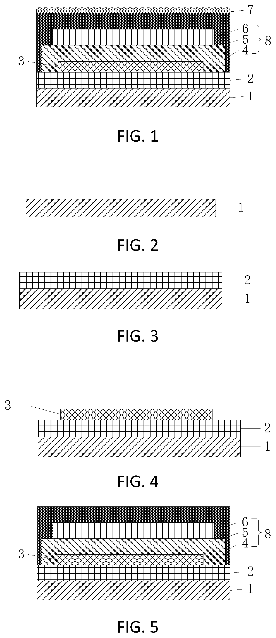
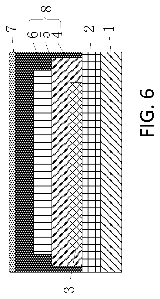
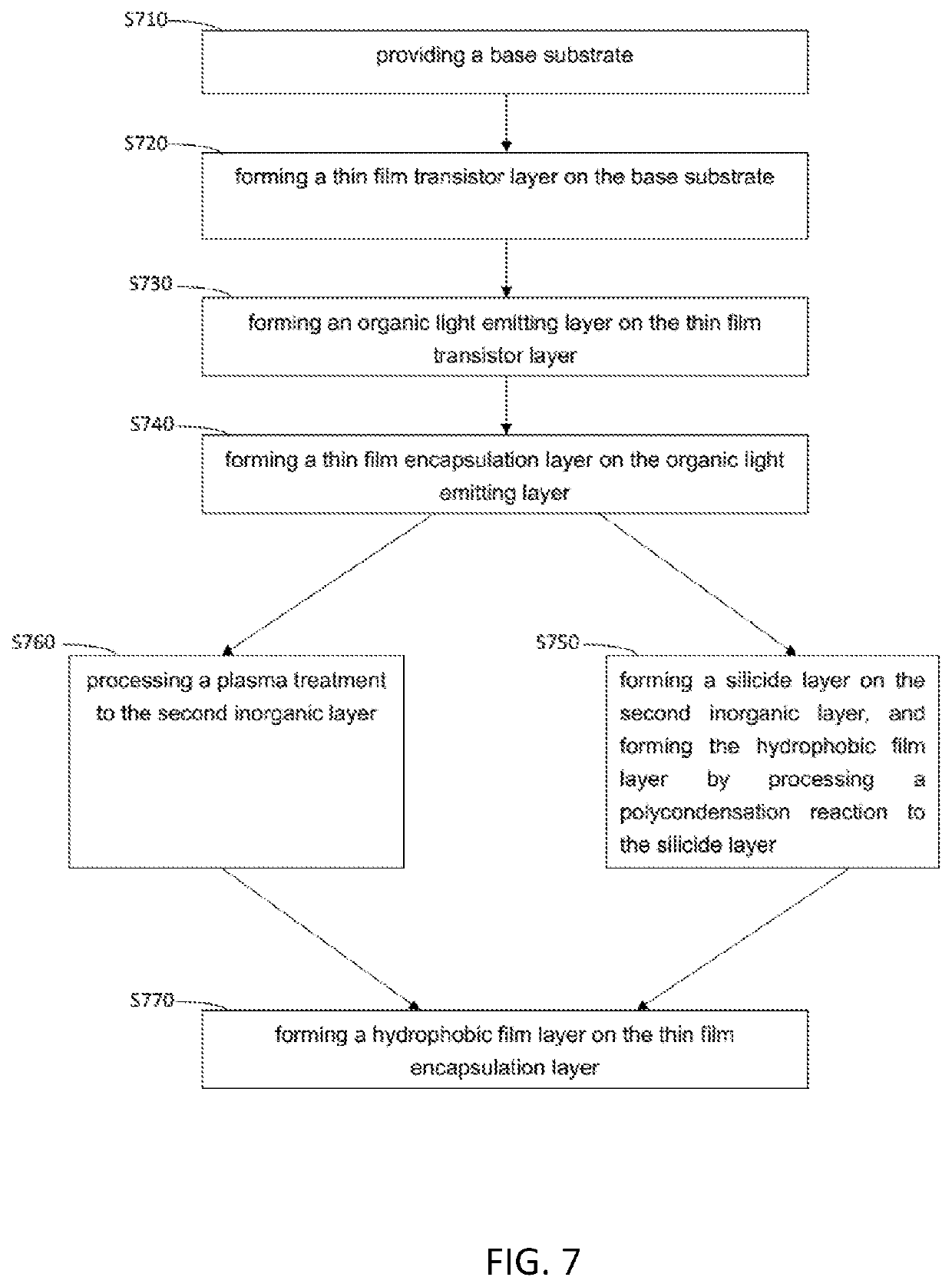

Image

  • Organic light emitting diode display panel and manufacturing method thereof, and display device
  • Organic light emitting diode display panel and manufacturing method thereof, and display device
  • Organic light emitting diode display panel and manufacturing method thereof, and display device

Examples


Embodiment Construction

[0032]The technical solutions in the embodiments of the present disclosure are clearly and completely described below. It is obvious that the described embodiments are not all the embodiments of the present disclosure. All other embodiments obtained by those skill in the art without inventive steps are within the protective scope of the present disclosure.

[0033]In the description of the present disclosure, it is to be understood that the terms of orientation or positional relationship such as “center”, “longitudinal”, “transverse”, “length”, “width”, “thickness”, “upper”, “lower”, “front”, “rear”, “left”, “right”, “vertical”, “horizontal”, “top”, “bottom”, “inner”, “out”, “clockwise” or “counterclockwise” is based on the orientation or positional relationship shown in the figures, only for the convenience of describing the present disclosure and simplifying the description. Which is not intended to indicate or imply that the device or component referred to has a specific orientation...


PUM

PropertyMeasurementUnit
contact angleaaaaaaaaaa
hydrophobicaaaaaaaaaa
microstructureaaaaaaaaaa

Abstract

The present disclosure discloses an organic light emitting diode display panel, a method of manufacturing an organic light emitting diode display panel, and a display device. By forming a film layer having super-hydrophobic properties of the outer water oxygen barrier layer of the thin film encapsulation layer, that is, constructing a rough surface, the surface of the hydrophobic film layer has an extremely thin air layer to reduce direct contact of moisture with the thin film encapsulation layer, thereby reducing the penetration of water and oxygen effectively, improving the water-blocking ability of the film encapsulation layer, and extending the lifetime of the display panel.

Description

FIELD OF INVENTION[0001]The present disclosure relates to the field of display technologies, and more particularly to an organic light emitting diode display panel and manufacturing method thereof, and a display device.BACKGROUND OF INVENTION[0002]With the development of display technology, flexible display devices have wider applications due to their advantages of being light weight, thin thickness, flexibility, and wide viewing angle range. However, organic light emitting diode (OLED) materials are very sensitive to water and oxygen, and a small amount intrusion of water and oxygen will cause rapid decay of the device, affecting lifetime of the OLED. In order to ensure the lifetime of the flexible display device, the packaging technology is particularly important.[0003]In order to implement the flexible display of the OLED, the OLED protection is generally implemented using thin-film encapsulation (TFE). Current thin film encapsulation process is briefly as follows: (1) depositing...

Claims


Application Information

Patent Timeline
Patent Type & Authority Applications(United States)
IPC IPC(8): H01L27/32H01L51/52H01L51/56
CPCH01L27/3244H01L2227/323H01L51/56H01L51/5253H10K59/12H10K59/1201H10K59/8731H10K50/844H10K71/00
Inventor LU, RUIYAN, ZIJUN
Owner WUHAN CHINA STAR OPTOELECTRONICS SEMICON DISPLAY TECH CO LTD
Learn More