Display device

a display device and display technology, applied in the field of display devices, can solve the problems of not so fast response time, high energy consumption, and low efficiency of backlight units, and achieve the effects of fast response speed, reduced wiring, and increased possibility of proper alignmen

Active Publication Date: 2021-02-25
LG ELECTRONICS INC
View PDF0 Cites 3 Cited by
  • Summary
  • Abstract
  • Description
  • Claims
  • Application Information

AI Technical Summary

Benefits of technology

This patent aims to provide several technical effects. Firstly, it reduces the likelihood of neighboring light-emitting devices in a pixel region by improving the matching of a light-emitting structure and a substrate. Secondly, it reduces the likelihood of faulty or improper electrical connections between a light-emitting device and a lower wiring even when the light-emitting structure is rotated on an axis perpendicular to the substrate due to the shape of the light-emitting structure. Thirdly, it increases the possibility of proper alignment of the light-emitting device using a capillary force and a magnetic force by providing a magnetic portion and a reaction portion on the lower substrate and the light-emitting device. Fourthly, it allows for a high-speed screen with a fast response speed by disposing an inorganic light-emitting device in a pixel region. Fifthly, it eliminates the need for a separate backlight unit, providing excellent luminance and high efficiency. Lastly, it utilizes an inorganic material for the light-emitting device, which has a long lifespan.

Problems solved by technology

However, a liquid crystal displays (LCD) has some drawbacks, such as a not-so-fast response time and high energy consumption as it lowers efficiency of backlight unit with high efficiency.
In the case of an organic light emitting diode (OLED), organics have much shorter lifetimes of up to around 2 years as they are vulnerable to reliability, and have low mass-production yield.
However, in a large display device using such micro LEDs, there is a difficulty in aligning each of the micro LEDs to a lower wiring on which the respective pixel regions are located, due to their small size.
However, as the capillary force is too weak, a possibility of self-alignment is low.
As a result, many micro LEDs are wasted, which leads to a decrease in yield.

Method used


Image

  • Display device
  • Display device
  • Display device

Examples


first embodiment

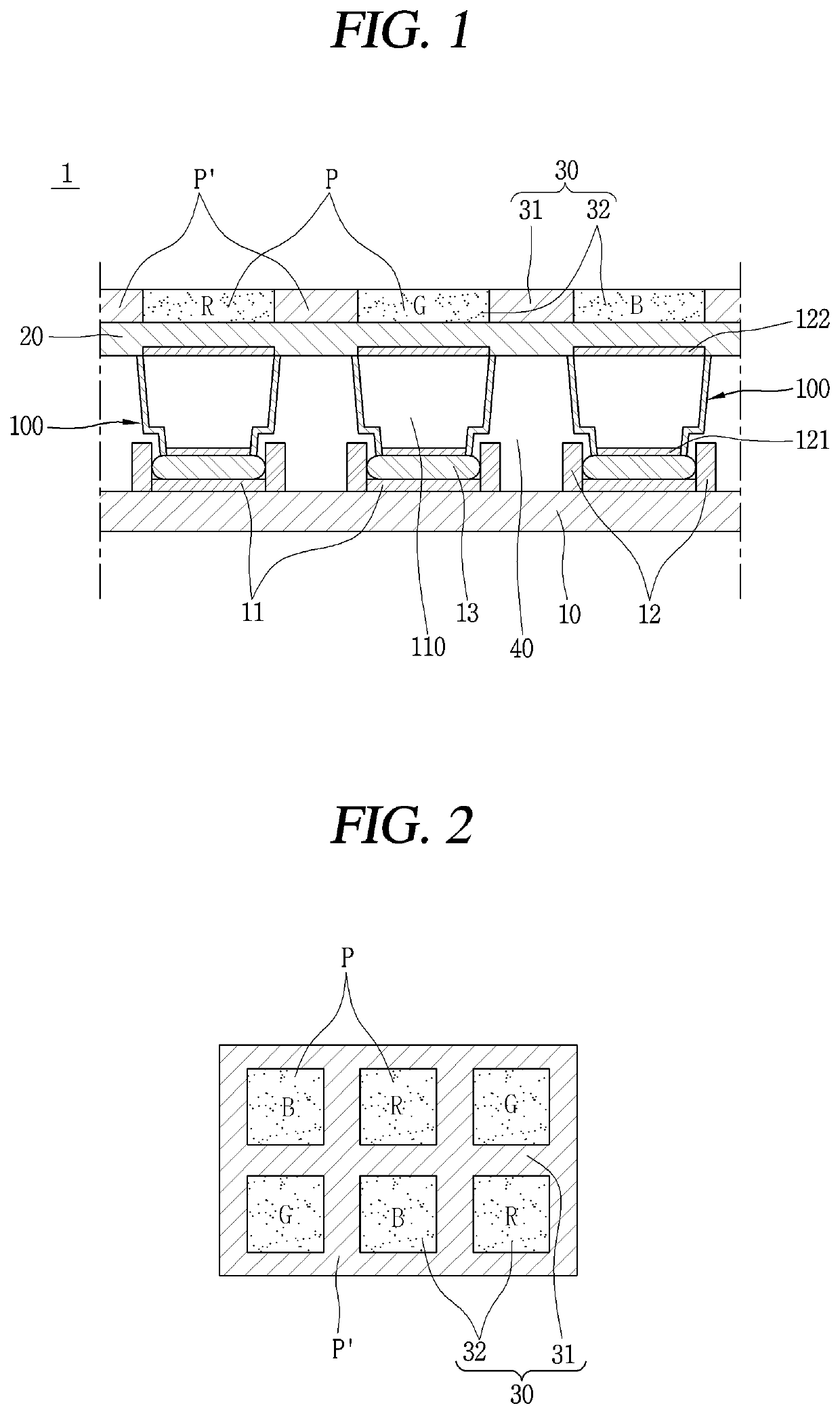
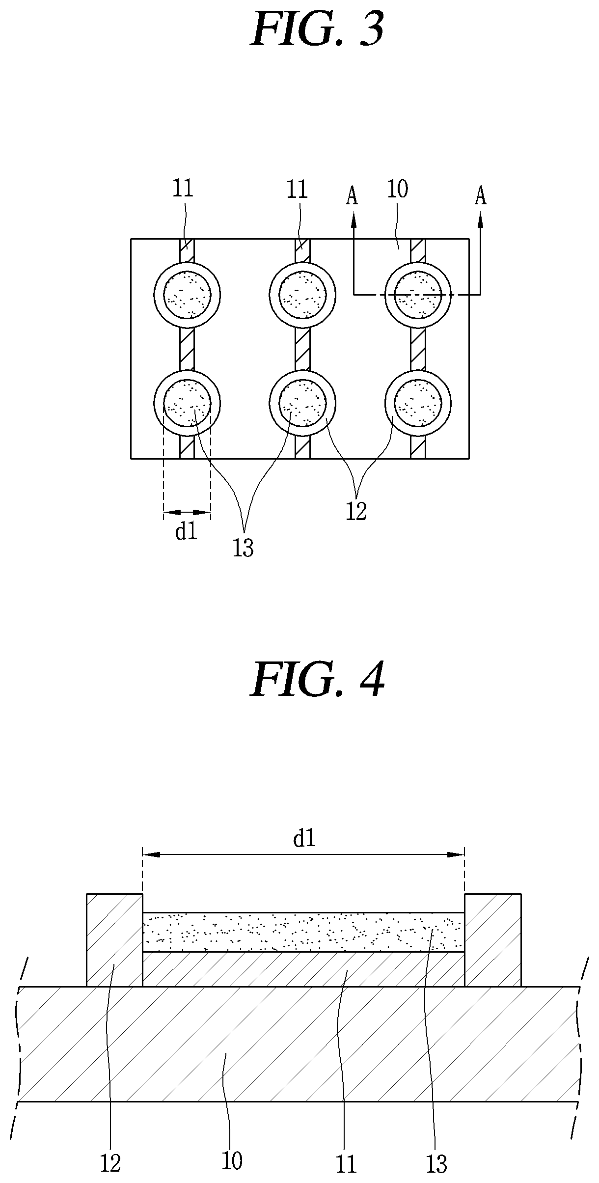
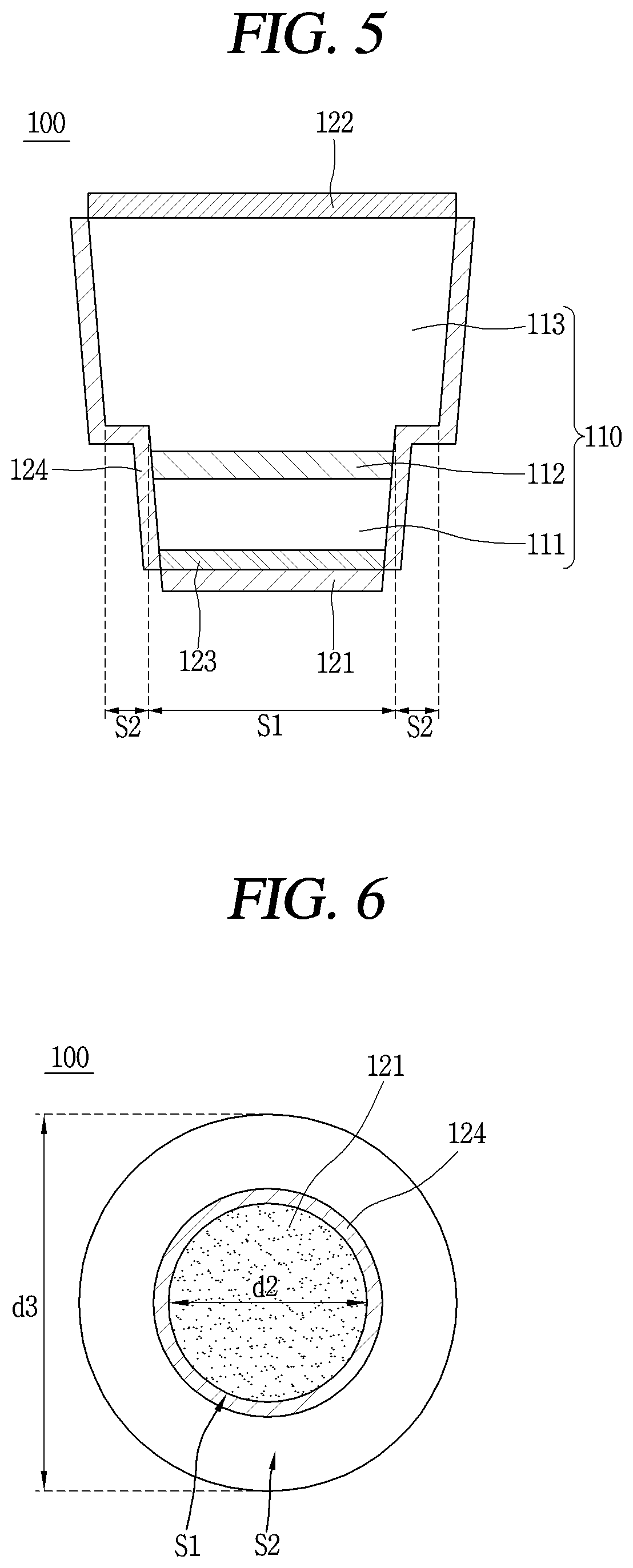
[0057]Referring to FIGS. 1 to 4, a display device 1 includes a lower substrate 10 on which lower wiring 11 is disposed, and at least two light-emitting devices (or elements) 100 each having a first electrode 121 electrically connected to the lower wiring 11 and a light-emitting structure 110 configured to generate light.

[0058]In addition, the display device 1 according to the first embodiment further includes a second electrode 122 located on a second conductive semiconductor layer 113, an upper wiring 20 electrically connected to the second electrode 122, and a color substrate 30 disposed on the light-emitting device 100 to convert a wavelength of light generated from the light-emitting device 100.

[0059]The lower substrate 10 may be implemented as a film made of an insulating material. For example, the lower substrate 10 may be made of a transparent glass material, or may be made of a transparent plastic or a polymer film having high flexibility.

[0060]The lower wiring 11 is dispos...

second embodiment

[0152]The display device 1A includes the lower substrate 10 on which at least two lower wirings 11 are disposed, at least two light-emitting devices 100A each having the first electrode 121 electrically connected to the lower wiring 11 and the light-emitting structure 110 that generates light, and the magnetic portion located on any one of the light-emitting device 100A and the lower substrate 10, and the reaction portion located on the remaining one, so as to be attracted by the magnetic portion.

[0153]In the second embodiment, the positioning partition wall 12 of the first embodiment is not provided. In the second embodiment, one light-emitting device 100A is self-aligned in one pixel region P by a magnetic force acting between the magnetic portion and the reaction portion.

[0154]The metal bonding layer 13 is disposed on the lower wiring 11 in an area where the light-emitting device 100A is to be located, as in the first embodiment.

[0155]The light-emitting device 100A of the second...

third embodiment

[0174]FIG. 13 is a cross-sectional view of a display device according to the present disclosure.

[0175]Referring to FIG. 13, a display device 1B according to the third embodiment further includes a second magnetic portion 15 and a second magnetic electrode 132, as compared to the second embodiment.

[0176]The magnetic portion may include the first magnetic portion 14 and the second magnetic portion 15, or include only the second magnetic portion 15 or only the first magnetic portion 14. In FIG. 13, the magnetic portion includes the first magnetic portion 14 and the second magnetic portion 15.

[0177]When a magnetic force of the magnetic portion is weak, a possibility of proper alignment of the light-emitting device 100A decreases, and thus a plurality of magnetic portions may be provided. That is, a plurality of magnetic portions is provided in one pixel region P.

[0178]The second magnetic portion 15 is located at the lower surface of the lower substrate 10. In detail, the second magnetic...


PUM


Abstract

Discussed is a display device including a lower substrate on which a lower electrode is disposed; a flat layer disposed on the lower substrate and having a plurality of holes; a plurality of light-emitting devices respectively disposed in of the plurality of holes; a magnetic portion disposed on the lower substrate and having an magnetic property; and a reaction portion disposed at each of the plurality of light-emitting devices and forming an attractive force with the magnetic portion, wherein a magnetization direction of the magnetic portion is perpendicular to the lower substrate.

Description

TECHNICAL FIELD[0001]The present disclosure relates to a display device.BACKGROUND ART[0002]Recently, a flat panel display device having excellent features such as thin and light designs, and low power consumption has been widely developed and used in various fields.[0003]A liquid crystal display (LCD) is widely used in various areas, from small-sized portable terminals to large-sized televisions, because of its high display quality and features such as thin and lightweight designs, and low power consumption.[0004]An organic light emitting diode (OLED) display device (hereinafter, “OLED”) is a device that emits light. Electrons and holes (electron holes) are injected into an emissive (or light-emitting) layer formed between a cathode which is an electron injection electrode and an anode which is a hole injection electrode. As the electrons and holes recombine, electron-hole pairs are created, forming an exciton. The emissive layer emits light as the excited state decays. Such an OLE...

Claims


Application Information

Patent Timeline
IPC IPC(8): H01L25/075H01L33/50H01L33/62
CPCH01L25/0753H01L33/505H01L2933/0066H01L2933/0041H01L33/62H01L33/38H01L33/40H01L27/156
Inventor JEON, KISEONG
Owner LG ELECTRONICS INC
Why Eureka
Try Eureka