Methods for selective deposition using a sacrificial capping layer

a selective deposition and capping layer technology, applied in chemical vapor deposition coatings, coatings, semiconductor devices, etc., can solve the problems of inability to selectively deposit a relatively low contact resistance boron-doped silicon germanium layer, difficulty in techniques, and low contact resistance of boron-doped silicon germanium films. achieve the effect of improving contact resistance and low contact resistan

Active Publication Date: 2021-03-04
ASM IP HLDG BV
View PDF0 Cites 151 Cited by
  • Summary
  • Abstract
  • Description
  • Claims
  • Application Information

AI Technical Summary

Benefits of technology

[0008]Various embodiments of the present disclosure relate to selective deposition methods, to structures and devices formed using such methods, and to apparatus for performing the methods and / or for forming the structure and / or devices. While the ways in which various embodiments of the present disclosure address drawbacks of prior methods and systems are discussed in more detail below, in general, various embodiments of the disclosure provide improved methods of selectively depositing a p-type doped silicon germanium layer. The p-type doped silicon germanium layer can exhibit relatively low contact resistance. Additionally or alternatively, the p-type doped silicon germanium layer can be formed at relatively low temperatures—e.g., 350° C. to 600° C., without the use of a step of annealing the p-type doped silicon germanium layer to improve the contact resistance of the p-type doped silicon germanium layer.

Problems solved by technology

While boron-doped silicon germanium films may work well in some applications, the contact resistance of the boron-doped silicon germanium films may be undesirably high, particularly for use as source / drain regions in field effect transistors (FET).
Such techniques may be problematic because the use of the relatively high temperatures during the anneal process can lead to clustering of one or more of the dopants of the doped silicon germanium films.
However, attempts to selectively deposit a p-type doped silicon germanium layer that has relatively low contact resistance have been challenging.

Method used


Image

  • Methods for selective deposition using a sacrificial capping layer
  • Methods for selective deposition using a sacrificial capping layer
  • Methods for selective deposition using a sacrificial capping layer

Examples


Embodiment Construction

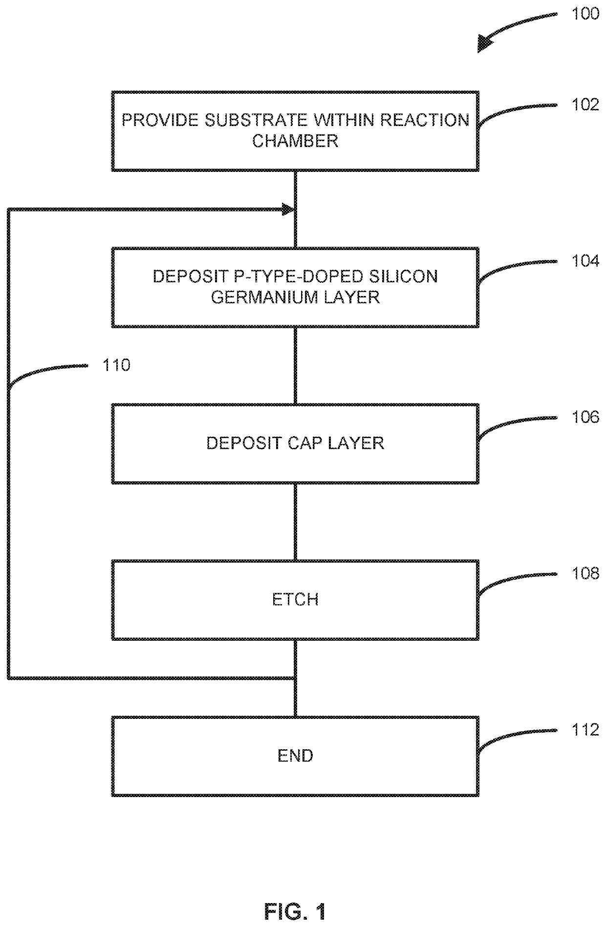
[0023]The description of exemplary embodiments of methods, structures, devices and systems provided below is merely exemplary and is intended for purposes of illustration only; the following description is not intended to limit the scope of the disclosure or the claims. Moreover, recitation of multiple embodiments having stated features is not intended to exclude other embodiments having additional features or other embodiments incorporating different combinations of the stated features.

[0024]As set forth in more detail below, various embodiments of the disclosure provide methods for selectively depositing a p-type doped silicon germanium layer including gallium. Exemplary methods can be used to, for example, form source or drain regions of semiconductor devices that exhibit relatively low contact resistance and that maintain the structure and composition of the p-type doped silicon germanium layer including gallium.

[0025]Typical solutions to deposit p-type doped silicon germanium l...


PUM

PropertyMeasurementUnit
thicknessaaaaaaaaaa
thicknessaaaaaaaaaa
thicknessaaaaaaaaaa

Abstract

Methods and systems for selectively depositing a p-type doped silicon germanium layer and structures and devices including a p-type doped silicon germanium layer are disclosed. An exemplary method includes providing a substrate, comprising a surface comprising a first area comprising a first material and a second area comprising a second material, within a reaction chamber; depositing a p-type doped silicon germanium layer overlying the surface, the p-type doped silicon germanium layer comprising gallium; and depositing a cap layer overlying the p-type doped silicon germanium layer. The method can further include an etch step to remove the cap layer and the p-type doped silicon germanium layer overlying the second material.

Description

CROSS-REFERENCE TO RELATED APPLICATIONS[0001]This application claims priority to U.S. Provisional Patent Application Ser. No. 62 / 895,819 filed Sep. 4, 2019 titled METHODS FOR SELECTIVE DEPOSITION USING A SACRIFICIAL CAPPING LAYER, the disclosures of which are hereby incorporated by reference in their entirety.FIELD OF INVENTION[0002]The present disclosure generally relates to methods and systems suitable for forming electronic devices. More particularly, the disclosure relates to methods and systems that can be used for selectively depositing a doped silicon germanium film on a surface of a substrate.BACKGROUND OF THE DISCLOSURE[0003]Because of their relatively high electron and / or hole mobility, high-mobility semiconductors, such as silicon germanium, may be desirable to use in the fabrication of electronic devices, such as semiconductor devices. Devices formed with high-mobility semiconductor materials may exhibit better performance, faster speeds, reduced power consumption, and h...

Claims


Application Information

Patent Timeline
Patent Type & Authority Applications(United States)
IPC IPC(8): H01L21/02H01L21/311H01L29/167
CPCH01L21/02532H01L21/02381H01L29/167H01L21/31105H01L21/02362H01L21/02579H01L21/0262H01L21/02639H01L21/02535H01L29/785H01L21/02636H01L21/3065C23C16/22C23C16/56
Inventor BARBOSA LIMA, LUCAS PETERSENKHAZAKA, RAMIXIE, QI
Owner ASM IP HLDG BV
Why Eureka
Try Eureka