
System and method for minimizing the effects of sensor orientation in smart optical monitoring systems
a technology of optical monitoring system and sensor orientation, applied in the field of additive manufacturing (am), can solve the problems of insufficient post-process quality assurance, both processes have relative strength and weaknesses, etc., and achieve the effect of minimizing the fluctuation of spectral signals
Patent Information
- Authority / Receiving Office
- US · United States
- Current Assignee / Owner
- Publication Date
- 2021-03-11
- Estimated Expiration
- Not applicable · inactive patent
Smart Images

Figure 1 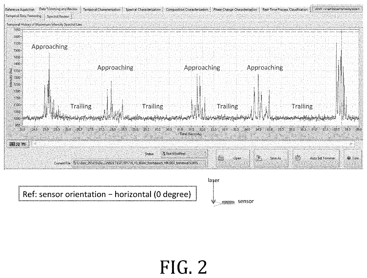
Figure 2 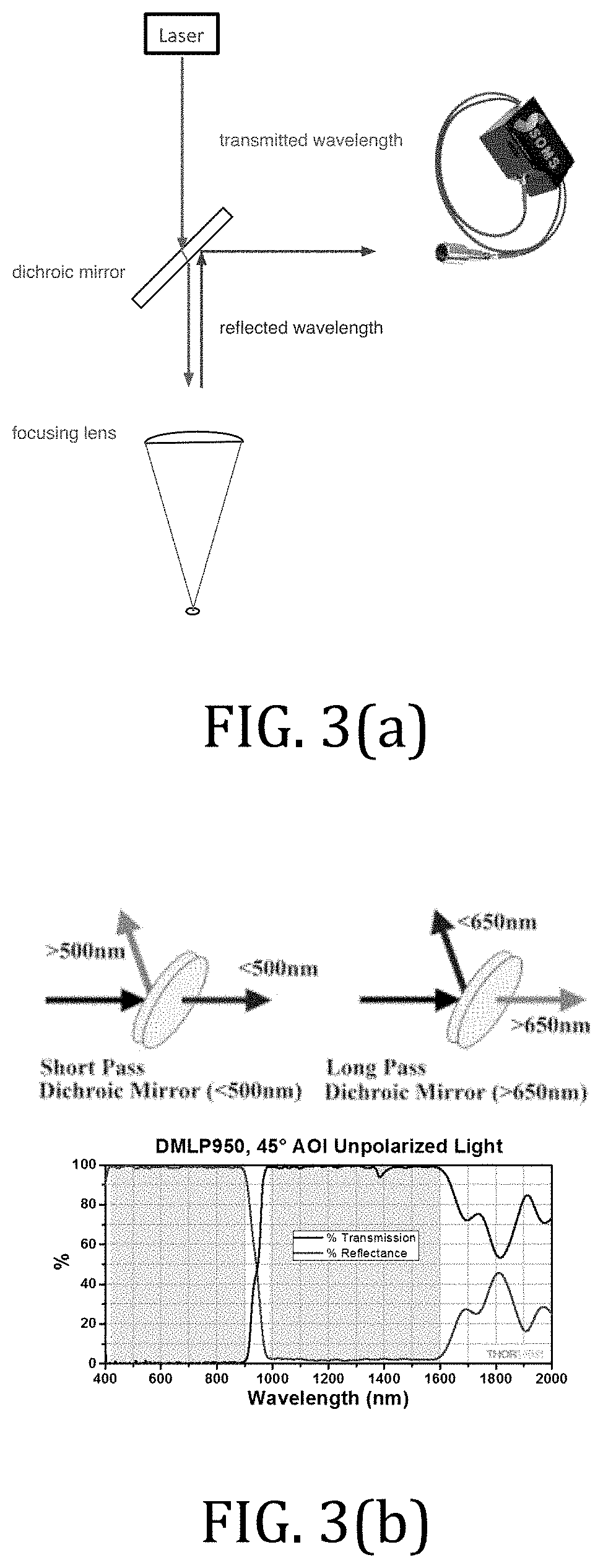
Figure 3
Abstract
Description
REFERENCE TO RELATED APPLICATIONS
[0001] This application claims priority to and the benefit of U.S. Provisional Patent Application Ser. No. 62 / 898,617, filed Sep. 11, 2019, the entire content of which is incorporated herein by reference.FIELD OF THE INVENTION
[0002] This invention relates generally to additive manufacturing (AM) and, in particular, to a smart AM system that uses an improved, co-axial laser / sensor path smart optical monitoring system (SOMS).BACKGROUND OF THE INVENTION
[0003] Additive manufacturing (AM) has been hailed as the “third industrial revolution” by Economist magazine (April 2012). Additive Manufacturing (AM) builds up a material to suit the service performance in a layer by layer, or even pixel by pixel with appropriate materials to match the performance, which will enhance the productivity and thus reduce energy consumption. Flexibility and capability of producing near net shape critical components directly from Computer Aided Design (CAD) is partly responsible ...
Examples
Embodiment Construction
[0016]To increase the accuracy of additive manufacturing (AM) in general, and direct-metal deposition (DMD); directed-energy deposition (DED); and powder-bed deposition systems in particular, a spectroscopic sensor may be used to achieve a Smart Optical Monitoring System (SOMS). This equipment, shown in FIG. 1(a), addresses many of the challenges faced by manufacturing industries, including stringent customer demands, intensified competition to reduce lead time, cycle time and manual labor, and rigorous requirements to eliminate liability of defective products.
[0017]SOMS uses optical emission spectroscopy to improve manufacturing quality to achieve no-defect product throughput in metal manufacturing processes, especially laser / arc welding and additive manufacturing (AM) processes. SOMS has the ability to perform in-situ characterization of defects such as porosity, composition, and phase transformation for fabrication processes using emitted light without any physical contact.
[0018]...