Semiconductor device package

Pending Publication Date: 2021-04-15
ADVANCED SEMICON ENG INC
View PDF7 Cites 0 Cited by
  • Summary
  • Abstract
  • Description
  • Claims
  • Application Information

AI Technical Summary

Benefits of technology

The present disclosure provides a semiconductor device package that includes a semiconductor device, an electrical conductor for electrical connection, and a redistribution structure for electrical connection between the semiconductor device and the electrical conductor. The redistribution structure includes dielectric layers stacked on each other, with a larger size dielectric layer adjacent to the electrical conductor. The semiconductor device package also includes conductive regions and a first dielectric region that connect the circuit layers corresponding to the dielectric layers. The technical effect of the present disclosure is to improve the efficiency and reliability of semiconductor device packages by providing a more reliable electrical connection between the semiconductor device and external devices.

Problems solved by technology

Such tests, however, may cause damage to a semiconductor package that includes the semiconductor chips.

Method used


Image

  • Semiconductor device package
  • Semiconductor device package
  • Semiconductor device package

Examples


Embodiment Construction

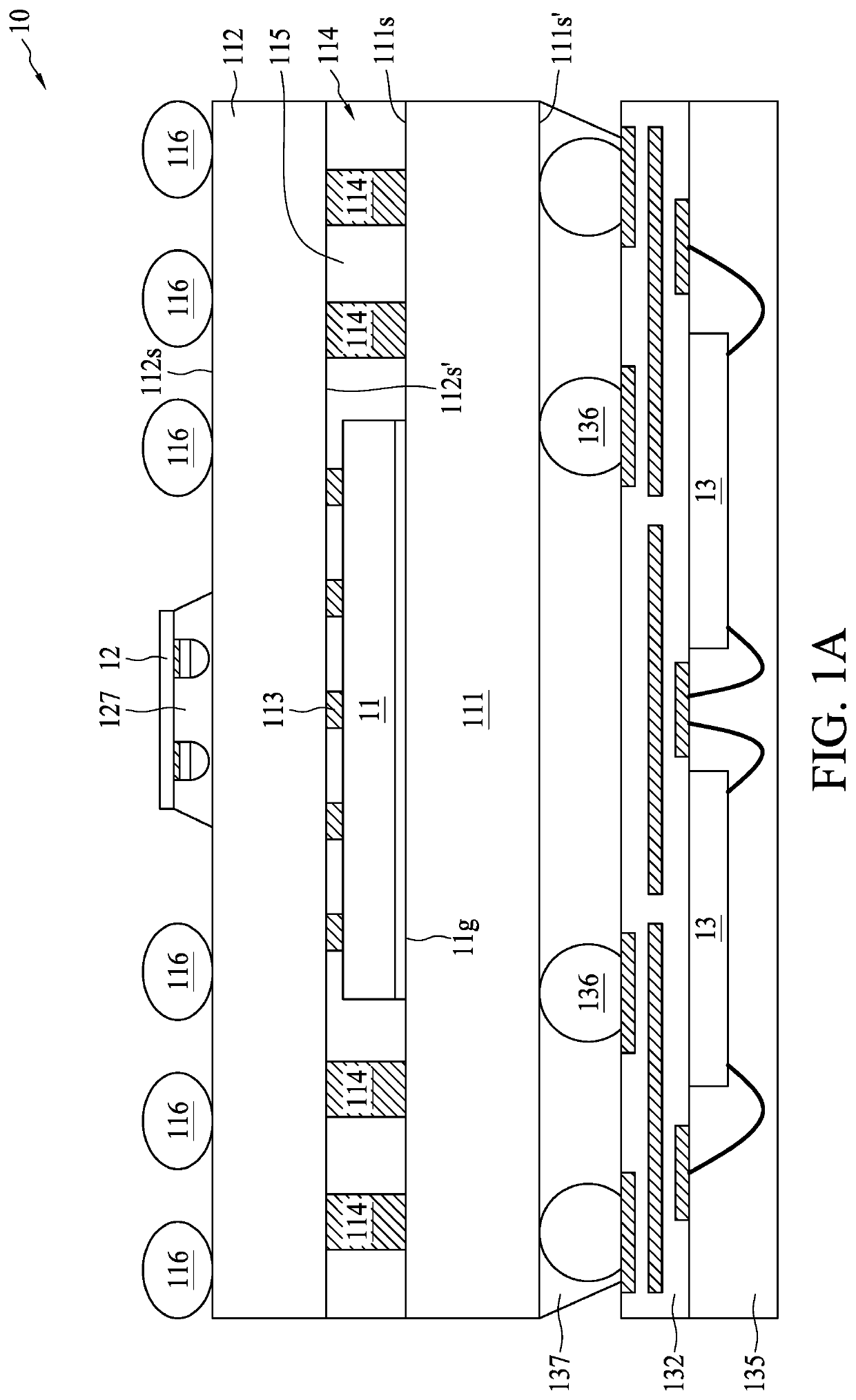
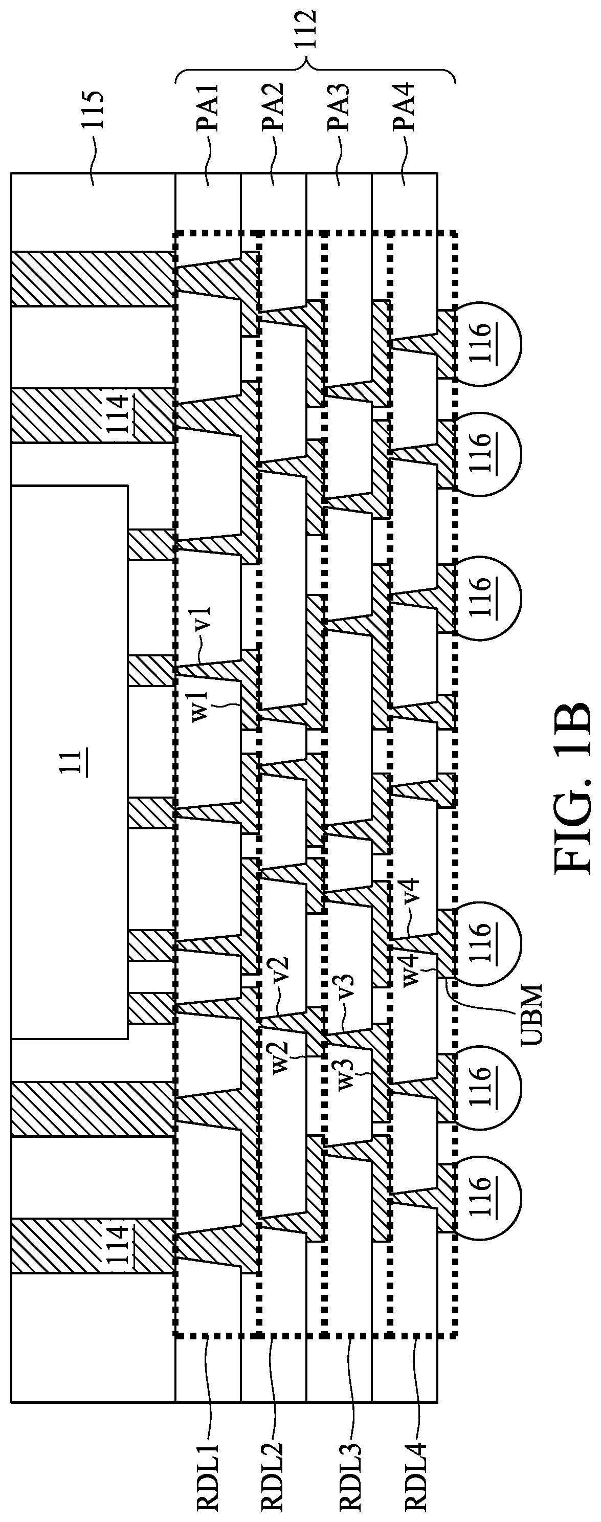
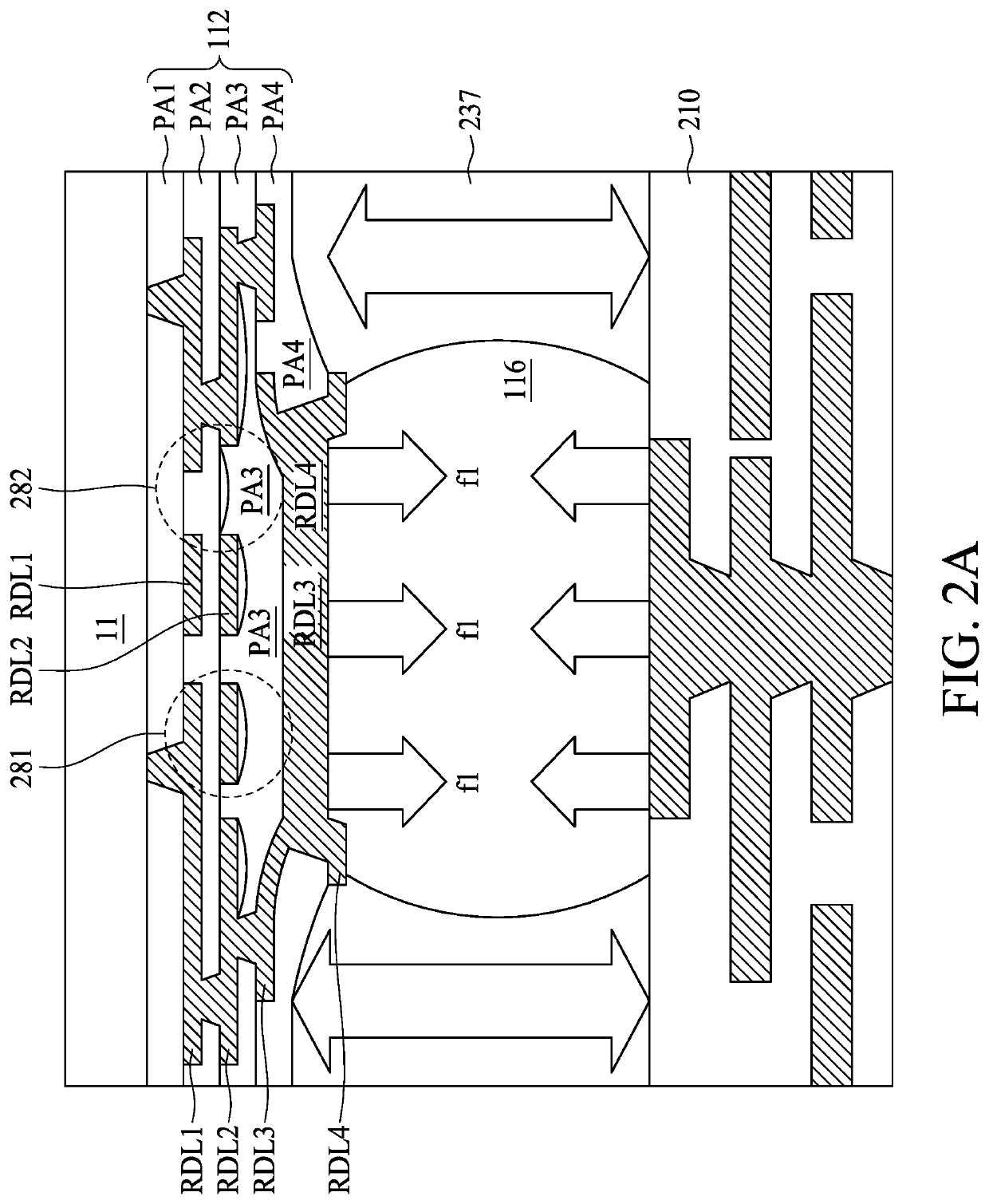
[0024]Common reference numerals are used throughout the drawings and the detailed description to indicate the same or similar components. Embodiments of the present disclosure will be readily understood from the following detailed description taken in conjunction with the accompanying drawings.

[0025]Spatial descriptions, such as “above,”“below,”“up,”“left,”“right,”“down,”“top,”“bottom,”“vertical,”“horizontal,”“side,”“higher,”“lower,”“upper,”“over,”“under,” and so forth, are specified with respect to a certain component or group of components, or a certain plane of a component or group of components, for the orientation of the component(s) as shown in the associated figure. It should be understood that the spatial descriptions used herein are for purposes of illustration only, and that practical implementations of the structures described herein can be spatially arranged in any orientation or manner, provided that the merits of embodiments of this disclosure are not deviated from by ...


PUM


Abstract

A semiconductor device package includes a semiconductor device in an encapsulating layer, an electrical conductor for electrical connection of the semiconductor device to an external device, and a redistribution structure for electrical connection between the semiconductor device and the electrical conductor. The redistribution structure includes dielectric layers stacked on each other in a direction extending between the encapsulating layer and the electrical conductor, wherein the dielectric layer most adjacent to the electrical conductor includes a first pattern under the electrical conductor, and circuit layers each corresponding to a respective one of the dielectric layers. The semiconductor device package further includes a conductive region disposed in the dielectric layer most adjacent to the electrical conductor according to the first pattern, and a first dielectric region, disposed in the dielectric layer most adjacent to the electrical conductor under the electrical conductor according to the first pattern, and surrounded by the conductive region.

Description

BACKGROUND1. Field of the Disclosure[0001]The present disclosure is generally related to semiconductor packaging and, in particular, to a semiconductor device package.2. Description of the Related Art[0002]Along with the rapid development in electronics industry and the progress of semiconductor processing technologies, semiconductor chips are integrated with an increasing number of electronic components to achieve improved electrical performance and additional functions. To ensure the desired performance and functions, electrical tests and / or reliability tests are performed for semiconductor chips during or after manufacturing. Such tests, however, may cause damage to a semiconductor package that includes the semiconductor chips.SUMMARY[0003]Embodiments of the present disclosure provide a semiconductor device package that includes a semiconductor device in an encapsulating layer, an electrical conductor for electrical connection of the semiconductor device to an external device, an...

Claims


Application Information

Patent Timeline
IPC IPC(8): H01L23/498H01L23/31H01L23/538H01L25/10
CPCH01L23/49822H01L23/3128H01L23/5389H01L24/16H01L25/105H01L2224/16225H01L23/5386H01L21/6835H01L21/568H01L2221/68327H01L2221/68354H01L2221/68359H01L2221/68372H01L2221/68318H01L25/50H01L25/18H01L21/563H01L23/564H01L2924/00014H01L2224/48091H01L2224/73253H01L2924/181H01L2224/32225H01L2224/73204H01L2924/19011H01L2924/19106H01L24/19H01L24/20H01L24/32H01L24/73H01L24/48H01L22/32H01L2225/1041H01L2225/1058H01L23/5385H01L23/49816H01L21/4853H01L2225/1035H01L25/16H01L2224/45099H01L2224/45015H01L2924/207H01L2924/00012H01L2224/29099H01L2224/13099H01L2924/00H01L2224/48228
Inventor CHOU, TING-YANG
Owner ADVANCED SEMICON ENG INC
Why Eureka
Try Eureka