Method of forming structures including a vanadium or indium layer

a technology of vanadium or indium layer and forming structure, which is applied in the direction of coating, transistor, chemical vapor deposition coating, etc., can solve the problems of reducing the number of carriers in the surface region, affecting the efficiency of the gate electrode, and affecting the performance of the gate electrod

Active Publication Date: 2021-08-05
ASM IP HLDG BV
View PDF0 Cites 120 Cited by
  • Summary
  • Abstract
  • Description
  • Claims
  • Application Information

AI Technical Summary

Benefits of technology

[0015]These and other embodiments will become readily apparent to those skilled in the art from the following detailed description of certain embodiments having reference to the attached figures. The invention is not being limited to any particular embodiments disclosed.

Problems solved by technology

However, conventional device scaling techniques face significant challenges for future technology nodes.
For example, one challenge has been finding a suitable conducting material for use as a gate electrode in the CMOS devices.
However, doped polysilicon may not be an ideal gate electrode material for advanced node applications.
Although doped polysilicon is conductive, there may still be a surface region which can be depleted of carriers under bias conditions.
As a further example, polysilicon does not exhibit an ideal effective work function (eWF) for both NMOS and PMOS devices.
However, as device geometries reduce in advanced node applications, the threshold voltage adjustment implantation processes may become increasingly complex and impractical.

Method used


Image

  • Method of forming structures including a vanadium or indium layer
  • Method of forming structures including a vanadium or indium layer
  • Method of forming structures including a vanadium or indium layer

Examples


Embodiment Construction

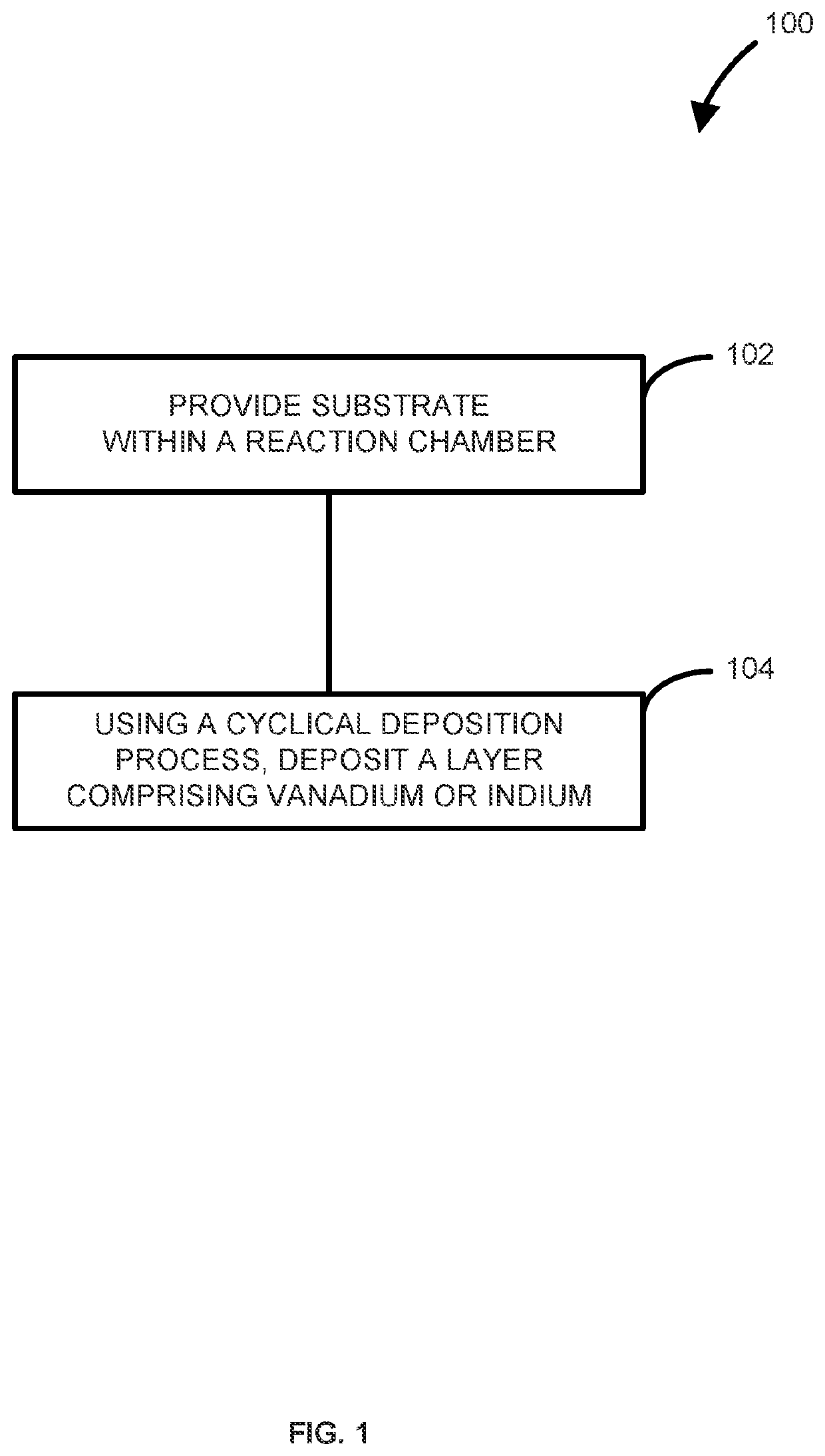
[0021]The description of exemplary embodiments of methods, structures, devices and systems provided below is merely exemplary and is intended for purposes of illustration only; the following description is not intended to limit the scope of the disclosure or the claims. Moreover, recitation of multiple embodiments having stated features is not intended to exclude other embodiments having additional features or other embodiments incorporating different combinations of the stated features. For example, various embodiments are set forth as exemplary embodiments and may be recited in the dependent claims. Unless otherwise noted, the exemplary embodiments or components thereof may be combined or may be applied separate from each other.

[0022]As set forth in more detail below, various embodiments of the disclosure provide methods for forming structures and / or devices suitable for a variety of applications. Exemplary methods can be used to, for example, form gate electrodes, and / or form van...


PUM

PropertyMeasurementUnit
thicknessaaaaaaaaaa
thicknessaaaaaaaaaa
temperatureaaaaaaaaaa

Abstract

Methods and systems for depositing vanadium and/or indium layers onto a surface of a substrate and structures and devices formed using the methods are disclosed. An exemplary method includes using a cyclical deposition process, depositing a vanadium and/or indium layer onto the surface of the substrate. The cyclical deposition process can include providing a vanadium and/or indium precursor to the reaction chamber and separately providing a reactant to the reaction chamber. The cyclical deposition process may desirably be a thermal cyclical deposition process. Exemplary structures can include field effect transistor structures, such as gate all around structures. The vanadium and/or indium layers can be used, for example, as barrier layers or liners, as work function layers, as dipole shifter layers, or the like.

Description

CROSS-REFERENCE TO RELATED APPLICATIONS[0001]This application in a non-provisional of, and claims priority to and the benefit of, U.S. Provisional Patent Application No. 62 / 969,504, filed Feb. 3, 2020 and entitled “METHOD OF FORMING STRUCTURES INCLUDING A VANADIUM OR INDIUM LAYER,” U.S. Provisional Patent Application No. 63 / 015,229, filed Apr. 24, 2020 and entitled “METHOD OF FORMING STRUCTURES INCLUDING A VANADIUM OR INDIUM LAYER,” and U.S. Provisional Patent Application No. 63 / 052,819 filed Jul. 16, 2020 and entitled “METHOD OF FORMING STRUCTURES INCLUDING A VANADIUM OR INDIUM LAYER,” which are hereby incorporated by reference herein.FIELD OF INVENTION[0002]The present disclosure generally relates to methods and systems suitable for forming a layer on a surface of a substrate and to structures including the layer. More particularly, the disclosure relates to methods and systems for forming layers that include vanadium and / or indium and to structures formed using the methods and sy...

Claims


Application Information

Patent Timeline
Patent Type & Authority Applications(United States)
IPC IPC(8): H01L21/02H01L29/423H01L27/092H01L29/06H01L29/66
CPCH01L21/0228H01L29/42392H01L21/02175H01L29/0669H01L29/66439H01L27/092H01L21/02172H01L21/02271C23C16/44C23C16/45527C23C16/36C23C16/308H01L21/02194H01L29/78H01L29/4966H01L29/4958H01L29/517H01L29/513H01L21/28556C23C16/06C23C16/18C23C16/45553H01L21/28088H01L21/76829
Inventor SHERO, ERIC JAMESGIVENS, MICHAEL EUGENEXIE, QIDEZELAH, CHARLESALESSIO VERNI, GIUSEPPE
Owner ASM IP HLDG BV
Why Eureka
Try Eureka