Heat flow switching element

a switching element and heat flow technology, applied in the direction of electrical equipment, semiconductor devices, semiconductor/solid-state device details, etc., can solve the problems of large influence of convective heat transfer between materials, difficult to design a size, and inability to avoid plastic deformation, etc., to achieve large change in thermal conductivity, reduce manufacturing cost and thickness, and high thermal responsiveness

Active Publication Date: 2021-08-12
MITSUBISHI MATERIALS CORP +1
View PDF0 Cites 0 Cited by
  • Summary
  • Abstract
  • Description
  • Claims
  • Application Information

AI Technical Summary

Benefits of technology

[0015]The present invention has been made in view of the above-described problems, and an object thereof is to provide a heat flow switching element which has a larger change in a thermal conductivity and has excellent thermal responsiveness.
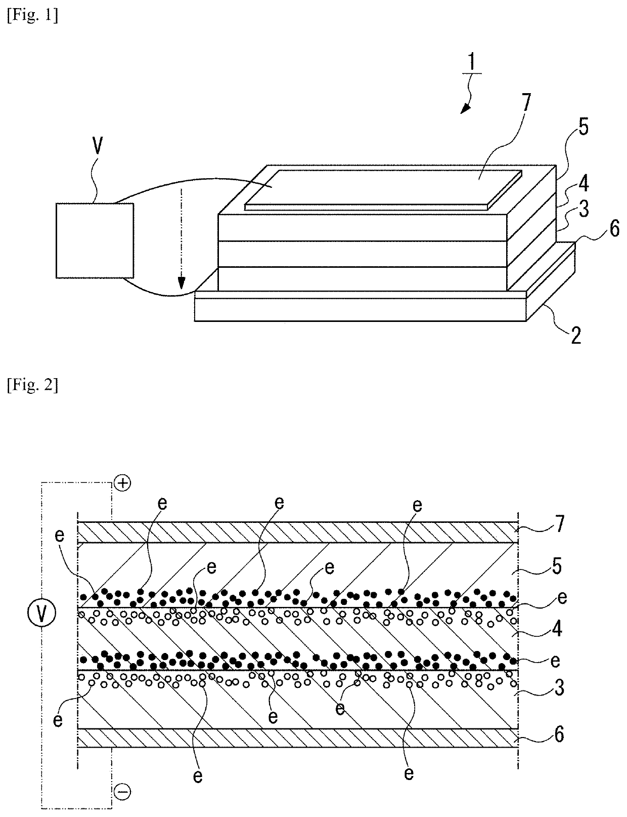
[0031]According to the present invention, the following effects can be obtained. That is, according to the heat flow switching element of the present invention, since the heat flow switching element includes an N-type semiconductor layer, an insulator layer laminated on the N-type semiconductor layer, and a P-type semiconductor layer laminated on the insulator layer, the amount of electric charges generated by application of an external voltage is large, and a large change in thermal conductivity and high thermal responsiveness can be obtained.

Problems solved by technology

The following problems remain in the above-described conventional technology.
That is, in the techniques described in Patent Documents 1 and 2, since the physical thermal contact due to the thermal expansion is used, reproducibility cannot be obtained, in particular, it is difficult to design a size due to a minute change, and it is not possible to avoid plastic deformation due to a mechanical contact pressure.
Also, there is a problem that an influence of convective heat transfer between materials is too large.
Further, in the technique described in Patent Document 3, there is a problem that an oxidation-reduction reaction which is a chemical reaction is used and thermal conduction is not stable due to poor thermal responsiveness.

Method used


Image

  • Heat flow switching element
  • Heat flow switching element
  • Heat flow switching element

Examples


example 1

[0094]An insulator layer, a P-type semiconductor layer, and a P-side electrode were laminated on an N-type semiconductor layer using the following materials to form Example 1 of the present invention, and a change in the thermal conductivity was measured.

[0095]N-type semiconductor layer: Si substrate of N-type semiconductor (thickness of 0.5 mm)

[0096]Insulator layer: SiO2 (thickness of 100 nm)

[0097]P-type semiconductor layer: Si0.375Ge0.575Au0.05 (thickness of 40 nm)

[0098]P-side electrode: Mo (thickness of 100 nm)

[0099]It has been confirmed that each of SiO2 (thickness of 100 nm) and Si0.375Ge0.575Au0.05 (thickness of 40 nm) has a thermal conductivity of less than 2 W / mK in a single film.

[0100]Further, SiO2 (thickness of 100 nm) was formed by an RF sputtering method, and Si0.375Ge0.575Au0.05 (thickness of 40 nm) was formed by an MBE method.

[0101]An Au wire was connected to the Si substrate of the N-type semiconductor and Mo of the P-side electrode, and a voltage was applied. Further...

example 2

[0103]An N-type semiconductor layer, an insulator layer, a P-type semiconductor layer, and a P-side electrode were laminated on a substrate using the following materials to form Example 2 of the present invention, and a change in the thermal conductivity was measured.

[0104]Substrate: glass substrate (thickness of 0.5 mm)

[0105]N-type semiconductor layer: Si0.36Ge0.56P0.08 (thickness of 40 nm)

[0106]Insulator layer: SiO2 (thickness of 30 nm)

[0107]P-type semiconductor layer: Si0.375Ge0.575Au0.05 (thickness of 20 nm)

[0108]P-side electrode: Mo (thickness of 100 nm)

[0109]It has been confirmed that each of Si0.36Ge0.56P0.08 (thickness of 40 nm), SiO2 (thickness of 30 nm) and Si0.375Ge0.575Au0.05 (thickness of 20 nm) has a thermal conductivity of less than 2 W / mK in a single film.

[0110]Further, SiO2 (thickness of 30 nm) was formed by an RF sputtering method, and Si0.36Ge0.56P0.08 (thickness of 40 nm) and Si0.375Ge0.575Au0.05 (thickness of 20 nm) were formed by an MBE method.

[0111]An Au wire ...


PUM

PropertyMeasurementUnit
thicknessaaaaaaaaaa
thicknessaaaaaaaaaa
thicknessaaaaaaaaaa

Abstract

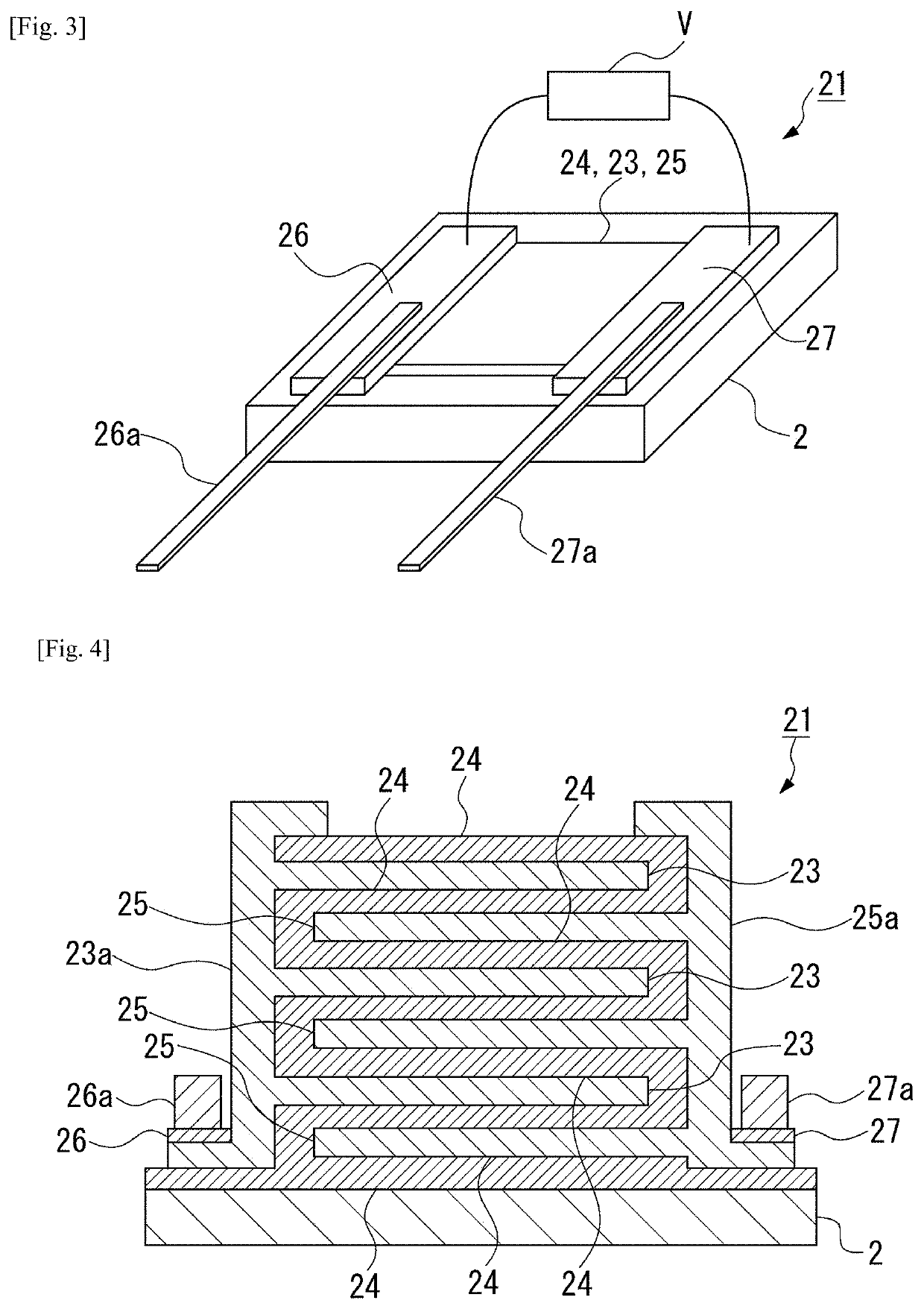
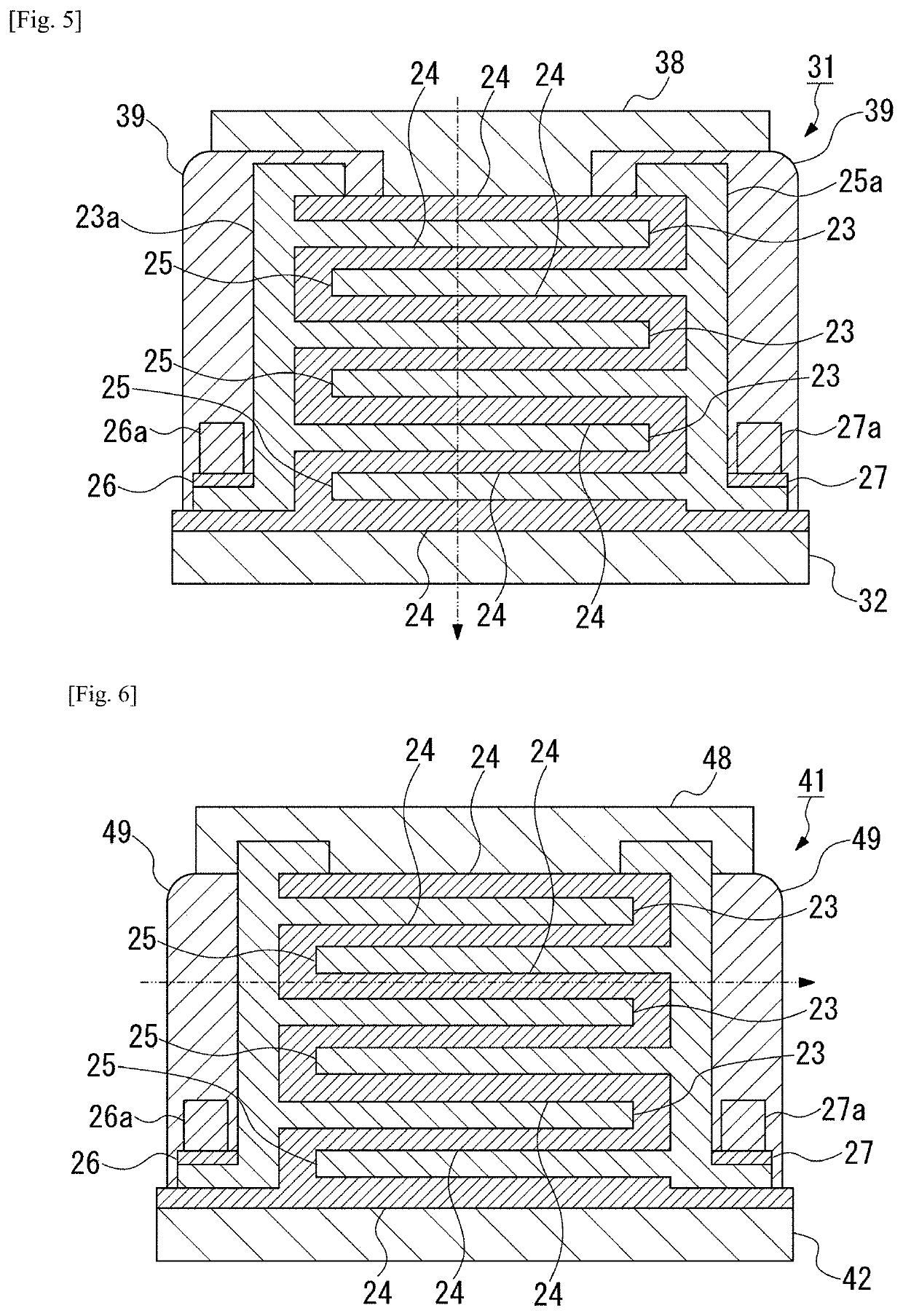
Provided is a heat flow switching element which has a larger change in a thermal conductivity and has excellent thermal responsiveness. The heat flow switching element includes an N-type semiconductor layer, an insulator layer laminated on the N-type semiconductor layer, a P-type semiconductor layer laminated on the insulator layer, an N-side electrode connected to the N-type semiconductor layer, and a P-side electrode connected to the P-type semiconductor layer. In particular, the insulator layer is formed of a dielectric. Also, a plurality of N-type semiconductor layers and P-type semiconductor layers are laminated alternately with the insulator layer interposed therebetween.

Description

BACKGROUND OF THE INVENTIONField of the Invention[0001]The present invention relates to a heat flow switching element which can actively control thermal conduction with a bias voltage.Description of Related Art[0002]Conventionally, as a thermal switch for changing a thermal conductivity, for example, Patent Document 1 discloses a thermal diode in which two thermal conductors having different thermal expansion coefficients are lightly brought into contact with each other to change a flow of heat depending on a direction of a temperature gradient.[0003]Further, Patent Document 2 also discloses a heat radiating device which is a thermal switch using physical thermal contact due to thermal expansion.[0004]Further, Patent Document 3 discloses a thermal conduction variable device in which a thermal conductivity is changed by a reversible oxidation-reduction reaction generated by applying a voltage to a compound.[0005]Furthermore, Non-Patent Document 1 proposes a heat flow switching elemen...

Claims


Application Information

Patent Timeline
Patent Type & Authority Applications(United States)
IPC IPC(8): H01L37/00H01H37/32H01L35/30H01L23/34H01L21/02
CPCH01L37/00H01H37/32H01L21/02642H01L23/34H01L21/02576H01L35/30H10N10/82H10N10/81H10N10/17H10N10/13H10N10/851H10N10/817
Inventor FUJITA, TOSHIAKIARAI, KOYATAKEUCHI, TSUNEHIROMATSUNAGA, TAKUYA
Owner MITSUBISHI MATERIALS CORP
Why Eureka
Try Eureka