Thin-film transistor array and method of producing the same

a technology of thin-film transistors and transistor arrays, which is applied in the direction of instruments, semiconductor devices, optics, etc., can solve the problem that the source and drain cannot be uniquely determined in thin-film transistors

Active Publication Date: 2021-08-26
TOPPAN PRINTING CO LTD
View PDF3 Cites 0 Cited by
  • Summary
  • Abstract
  • Description
  • Claims
  • Application Information

AI Technical Summary

Benefits of technology

The invention provides a thin-film transistor array that can save power when rewriting the display, and a method to produce this array.

Problems solved by technology

Thus, depending on the operation, sources and drains cannot be uniquely determined in thin-film transistors.

Method used


Image

  • Thin-film transistor array and method of producing the same
  • Thin-film transistor array and method of producing the same
  • Thin-film transistor array and method of producing the same

Examples


first embodiment

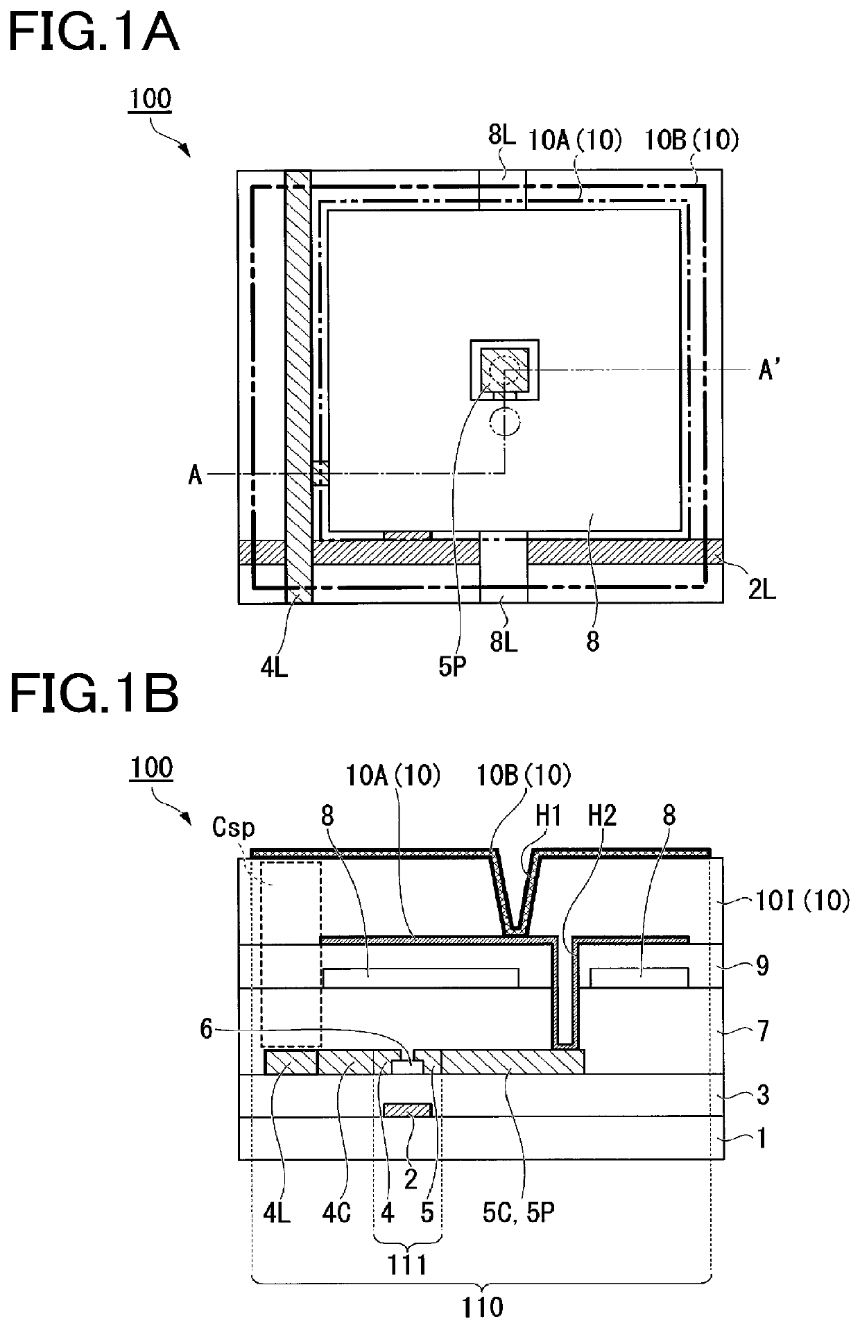
[0057]With reference to the drawing, some embodiments of the present invention will be described. FIGS. 1A and 1B are diagrams illustrating an example of a structure of a thin-film transistor array according to a first embodiment. In FIGS. 1A and 1B, the structure of the thin-film transistor array is schematically shown. Hereinafter, the thin-film transistor array is referred to as a thin-film transistor array 100. The thin-film transistor array 100 includes pixels each of which is provided with one thin-film transistor (TFT). Hereinafter, the thin-film transistor is referred to as a thin-film transistor 111, and each pixel is referred to as a pixel 110. More specifically, FIG. 1A is a schematic plan view showing a structure of a pixel 110 formed in the thin-film transistor array 100. FIG. 1B is a schematic cross-sectional view taken along the line A-A′ of the plan view of the pixel 110 shown in FIG. 1A. In the plan view of the pixel 110 shown in FIG. 1A, some components (lower pixe...

second embodiment

[0168]Next, a second embodiment of the present invention will be described. FIGS. 11A and 11B are diagrams illustrating an example of a structure of a thin-film transistor array according to a second embodiment of the present invention. FIGS. 11A and 11B schematically show a structure of a thin-film transistor array according to the second embodiment, as in FIGS. 1A and 1B showing the thin-film transistor array 100 according to the first embodiment. The thin-film transistor array according to the second embodiment is referred to as a thin-film transistor array 200 hereinafter. The thin film transistor array 200 includes pixels each of which is provided with one thin-film transistor. Hereinafter, the thin-film transistor is referred to as a thin-film transistor 211, and each pixel is referred to as a pixel 210. Specifically, FIG. 11A is a schematic plan view showing a structure of a pixel 210 formed in the thin-film transistor array 200. FIG. 1B is a schematic cross-sectional view ta...


PUM

PropertyMeasurementUnit
wavelengthaaaaaaaaaa
light transmittanceaaaaaaaaaa
relative permittivityaaaaaaaaaa

Abstract

A thin-film transistor array includes an insulating substrate and pixels each including a thin-film transistor, a pixel electrode, and a capacitor electrode, the pixels being formed in a matrix and located at positions where column wirings extending in a column direction intersect row wirings perpendicular to the column wirings and extending in a row direction. The thin-film transistor includes a gate electrode, a source electrode, a drain electrode, and a semiconductor pattern formed between the source electrode and the drain electrode. The pixel electrode includes two electrically conductive layers which are a lower layer electrode serving as a lower pixel electrode, and an upper layer electrode serving as an upper pixel electrode. The corresponding one of the column wirings is at a position which has no overlap with the capacitor electrode and the lower pixel electrode, and has an overlap with the upper pixel electrode, in the lamination direction.

Description

CROSS-REFERENCE TO RELATED APPLICATIONS[0001]The present application is a continuation of International Application No. PCT / JP2019 / 043377, filed Nov. 6, 2019, which is based upon and claims the benefits of priority to Japanese Application No. 2018-212157, filed Nov. 12, 2018. The entire contents of all of the above applications are incorporated herein by reference.BACKGROUND OF THE INVENTIONField of the Invention[0002]The present invention relates to thin-film transistor arrays and methods of producing the transistor arrays.Discussion of the Background[0003]Transistors using semiconductor substrates, or amorphous silicon (a-Si) or polysilicon (poly-Si) thin film transistor (TFT) arrays using glass substrates based on integrated circuit technology have been produced for application to liquid crystal display devices (liquid crystal displays) or other devices.[0004]Thin-film transistors serve as switches. Specifically, when a thin-film transistor is turned on by a selection voltage app...

Claims


Application Information

Patent Timeline
Patent Type & Authority Applications(United States)
IPC IPC(8): G02F1/1368G02F1/1362
CPCG02F1/1368G02F1/136213G02F1/136277G02F1/136286G02F1/167G02F1/16766H01L27/124
Inventor ISHIZAKI, MAMORU
Owner TOPPAN PRINTING CO LTD
Why Eureka
Try Eureka