Eureka AIR delivers breakthrough ideas for toughest innovation challenges, trusted by R&D personnel around the world.

Anisotropic conductive film

Pending Publication Date: 2021-09-30
DEXERIALS CORP
View PDF0 Cites 0 Cited by
  • Summary
  • Abstract
  • Description
  • Claims
  • Application Information

AI Technical Summary

Benefits of technology

The present invention relates to an anisotropic conductive film used in the production of flexible printed circuits. The film has a unique structure that prevents short circuits and improves the connection between terminals. The film has a wavy appearance which prevents conductive particles from close proximity and short circuits. The film also prevents irregular resin flows during thermocompression bonding and ensures uniform appearance of the terminals after connection. This results in improved efficiency and reliability of the flexible printed circuits.

Problems solved by technology

Therefore, there may be cases where the thermal expansion of the plastic substrate or FPC brings about a problem when the electronic components are mounted on such a substrate.

Method used


Image

  • Anisotropic conductive film
  • Anisotropic conductive film
  • Anisotropic conductive film

Examples


example

[0126]Hereinafter, the present invention will be described in detail with reference to Examples.

examples 1 to 5

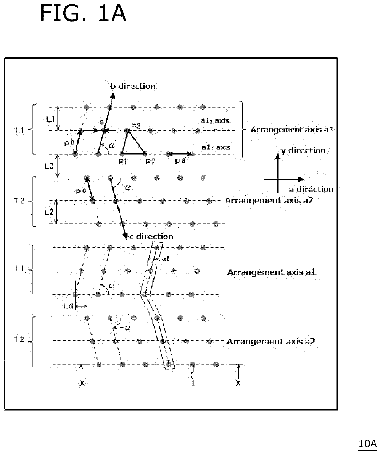
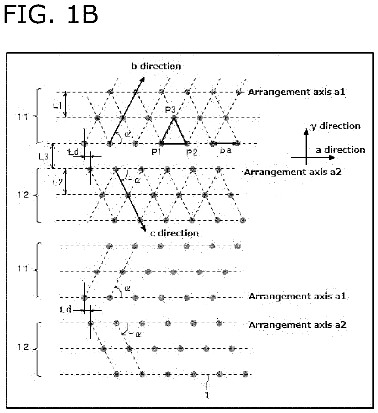
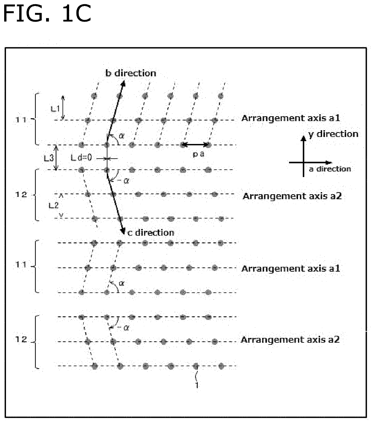
[0127]In the fan-out type terminal row A or B of each of specifications in Table 1, the following evaluation items (a) to (d) in the case of connecting the anisotropic conductive film with the particle disposition of each of Experimental Examples 1 to 5 shown in Table 2 were measured by simulation for evaluation. Among these, Experimental Examples 1 to 3 are examples of the present invention. Evaluation results are shown in Table 2. In relation to the evaluation results of (d), the simulation results of states of capturing the conductive particles in the terminal row B (the enlargement ratio of the inter-particle distances on a terminal and between terminals is also the same as in Table 1) when the number density was 16000 particles / mm2 in the disposition of the conductive particles in each of Experimental Examples 1, 3, 4, and 5 are shown in FIGS. 7A to 7D.

[0128]In this simulation, the x-direction which is the arrangement direction of the terminals and the a direction of the anisot...

experimental example 6

[0142]The disposition shown in FIG. 1K (L1=L2=L3: 7.5 μm, pitch pa: 8.4 μm, strain amount s: 2.1 μm, angle α: 75°, number density of particles: 16000 particles / mm2).


PUM


Abstract

An anisotropic conductive film in which conductive particles are disposed in an insulating resin layer has a particle disposition of the conductive particles such that a first orthorhombic lattice region being formed by arranging a plurality of arrangement axes of the conductive particles, disposed in an a direction at a predetermined pitch, in a b direction inclined with respect to the a direction at an angle, and a second orthorhombic lattice region being formed by arranging a plurality of arrangement axes of the conductive particles, disposed in the a direction at a predetermined pitch, in a c direction obtained by inverting the b direction with respect to the a direction are repeatedly disposed. Regardless of the shape of the terminal arrangements and the materials of electronic components, a good conduction state is ensured while the respective terminals hold conductive particles. Further, the occurrence of a short circuit is prevented.

Description

TECHNICAL FIELD[0001]The present invention relates to an anisotropic conductive film.BACKGROUND ART[0002]Weight reduction and flexibility have become required for substrates on which electronic components such as IC chips are to be mounted. For this reason, plastic substrates and FPCs (Flexible Printed Circuits) have been frequently used as substrates. In electronic components such as IC chips, terminal pitches are becoming finer. Therefore, there may be cases where the thermal expansion of the plastic substrate or FPC brings about a problem when the electronic components are mounted on such a substrate. Therefore, in order to reliably perform the connection of the electronic components even when the positions of the terminals are shifted due to the temperature fluctuation during mounting of the electronic components, respective terminals constituting a terminal row of the electronic components are radially arranged instead of being arranged in the same direction in the conventional...

Claims


Application Information

Patent Timeline
IPC IPC(8): H01L23/00
CPCH01L24/29H01L24/83H01L24/32H01L2924/301H01L2224/32145H01L2224/2957H01L2224/32225H01L2224/83203H01L2224/29005H01L2224/83851H01L2224/29082H01L2224/2939H01L2224/294H01L2224/293H01L2224/2929H01L2224/271H01L24/27H01L2224/83191H01L2224/83192H01L2224/83862H01L2224/83871H01L2224/83885H01L2224/81903H01L2224/9211H01L24/81H01L2224/81203H01L24/16H01L24/73H01L2224/73204H01L2224/16227H05K3/323H01L2224/29386H01L24/06H01L24/05H01L2224/04026H01L2224/0612H01L2224/05553H01L24/92H05K2201/0221H01L2224/27003H01L2224/2711H01L2224/29364H01L2224/29339H01L2224/29357H01L2224/29347H01L2224/29344H01L2224/29355H01L2924/381H01L2924/00014H01L2924/014H01L2924/00012H01L2224/81H01L2224/83H01L2924/05442H01L2924/0665H01L2224/16225H01L2924/00H01R11/01H01R43/00H05K3/32
Inventor TSUKAO, REIJITANIGUCHI, MASAKI
Owner DEXERIALS CORP
Why Eureka
Eureka Blog
Learn More