

Semiconductor device and method for manufacturing the same
a technology of semiconductor devices and semiconductor devices, applied in the direction of semiconductor devices, electrical equipment, transistors, etc., can solve the problems of permanent degradation of semiconductor devices, achieve the effects of reducing hot carrier electrons, and improving reliability problems of semiconductor devices
- Summary
- Abstract
- Description
- Claims
- Application Information
AI Technical Summary
Benefits of technology
Problems solved by technology
Method used
Image

Examples
Embodiment Construction
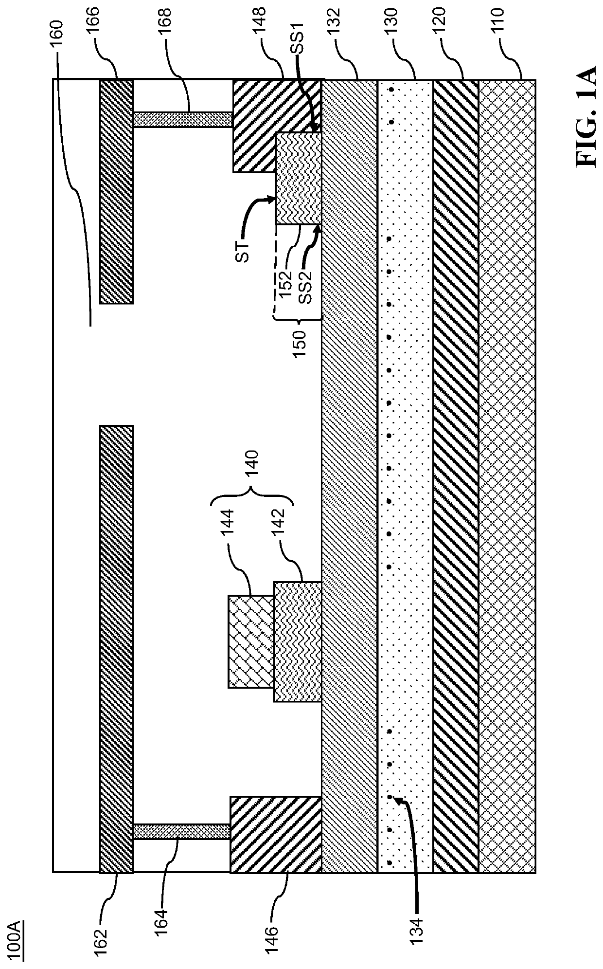
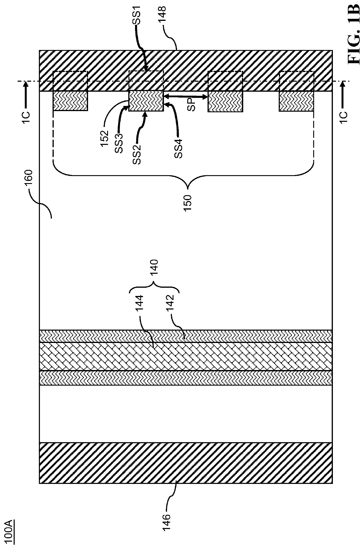
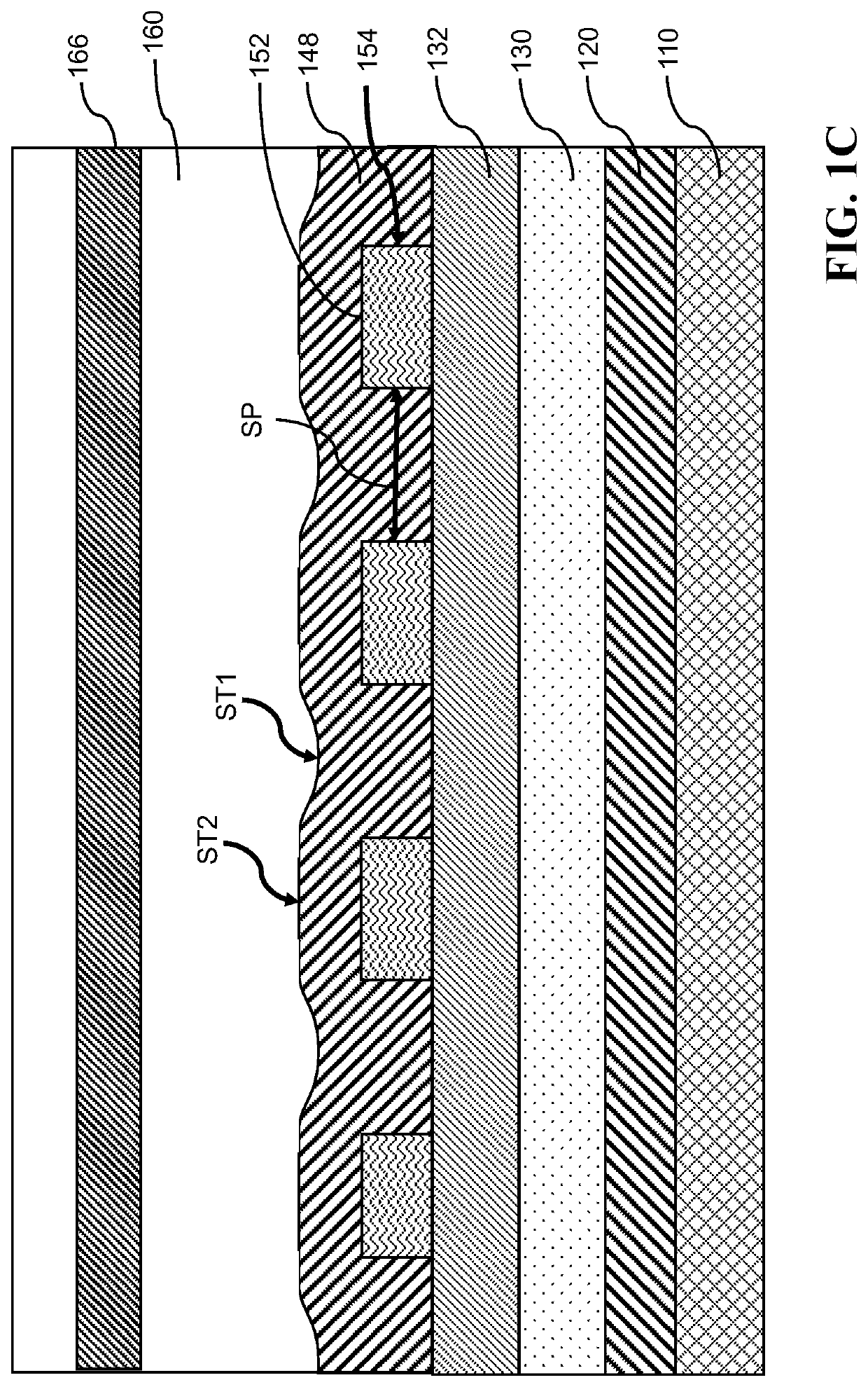
[0019]Common reference numerals are used throughout the drawings and the detailed description to indicate the same or similar components. Embodiments of the present disclosure will be readily understood from the following detailed description taken in conjunction with the accompanying drawings.
[0020]Spatial descriptions, such as “above,”“below,”“up,”“left,”“right,”“down,”“top,”“bottom,”“vertical,”“horizontal,”“side,”“higher,”“lower,”“upper,”“over,”“under,” and so forth, are specified with respect to a certain component or group of components, or a certain plane of a component or group of components, for the orientation of the component(s) as shown in the associated figure. It should be understood that the spatial descriptions used herein are for purposes of illustration only, and that practical implementations of the structures described herein can be spatially arranged in any orientation or manner, provided that the merits of embodiments of this disclosure are not deviated from by ...
PUM
| Property | Measurement | Unit |
|---|---|---|
| breakdown voltage | aaaaa | aaaaa |
| voltage | aaaaa | aaaaa |
| voltage | aaaaa | aaaaa |
Abstract
Description
Claims
Application Information