LED substrate and method for manufacturing LED display panel

Active Publication Date: 2021-11-18
SHENZHEN CHINA STAR OPTOELECTRONICS SEMICON DISPLAY TECH CO LTD
View PDF0 Cites 0 Cited by
  • Summary
  • Abstract
  • Description
  • Claims
  • Application Information

AI Technical Summary

Benefits of technology

[0057]Compared with the method for manufacturing micro-LED display panel of prior art, the method for manufacturing LED display panel of the present application forms a large-sized LED display panel directly, by first fixing the LED chips on the substrate to form an LED substrate, and then

Problems solved by technology

Currently, in the method for manufacturing a micro light-emitting diode (micro-LED) display panel, limited by influences of equipment precision and machine size, the manufacturing method is as follows: firstly, placing LEDs on a temporary substrate; secondly, grabbing the LEDs placed on the temporary substrate

Method used


Image

  • LED substrate and method for manufacturing LED display panel
  • LED substrate and method for manufacturing LED display panel
  • LED substrate and method for manufacturing LED display panel

Examples


first embodiment

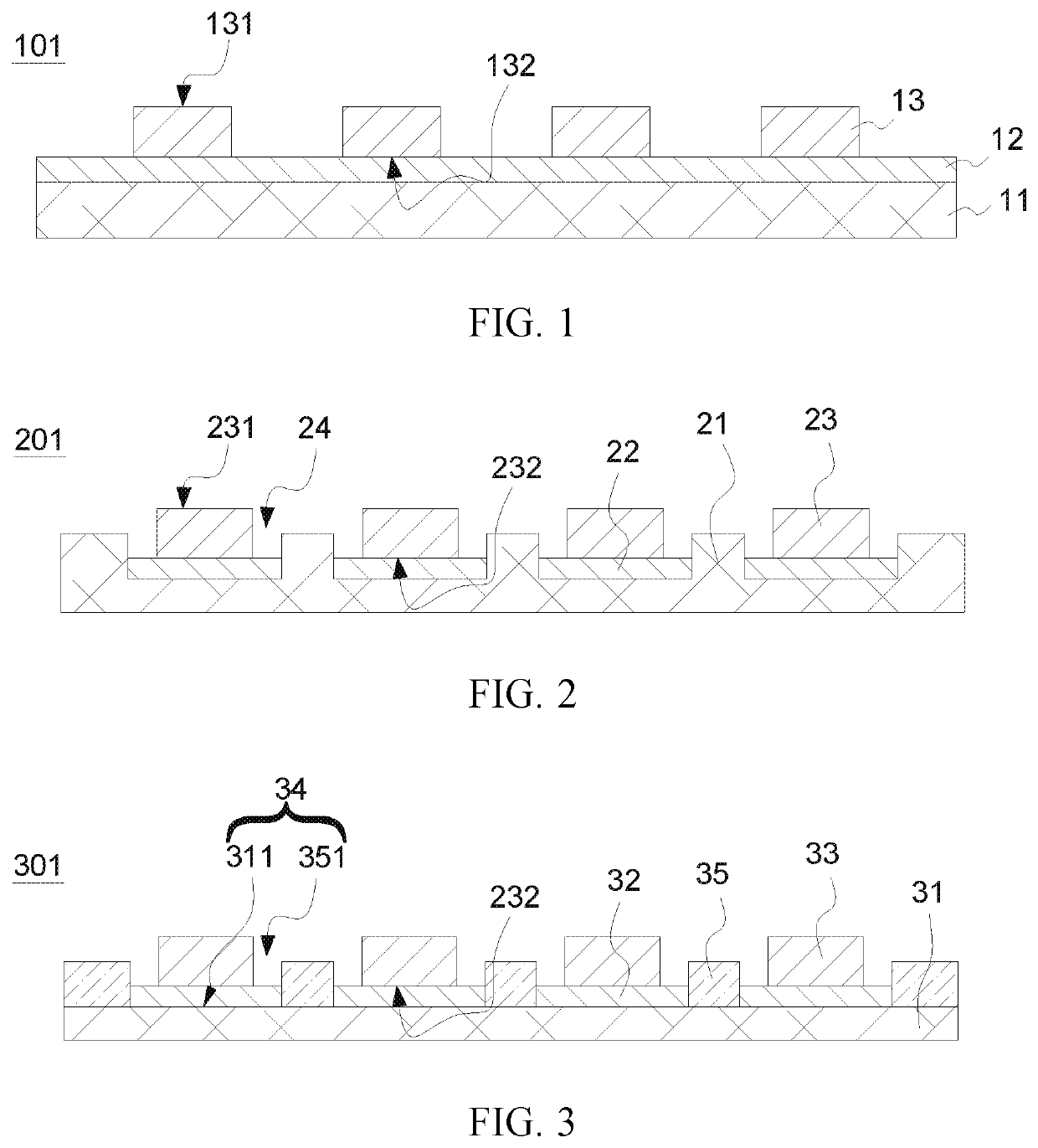
[0071]Please refer to FIG. 1, FIG. 1 is a structural schematic diagram of an LED substrate of the present application.

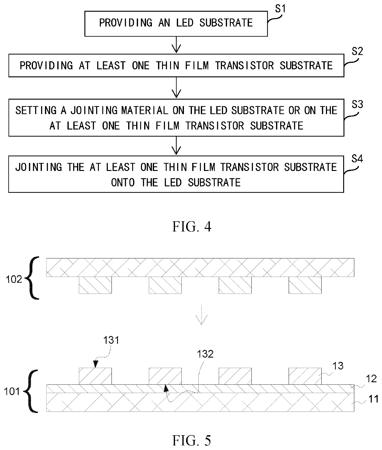
[0072]The LED substrate 101 in the first embodiment is for jointing with a plurality of thin film transistor substrates to form an LED display panel. Wherein, during a process of manufacturing the LED display panel, the plurality of thin film transistor substrates can be integrated onto the single LED substrate 101, and no further splicing is needed, which simplifies the manufacturing process.

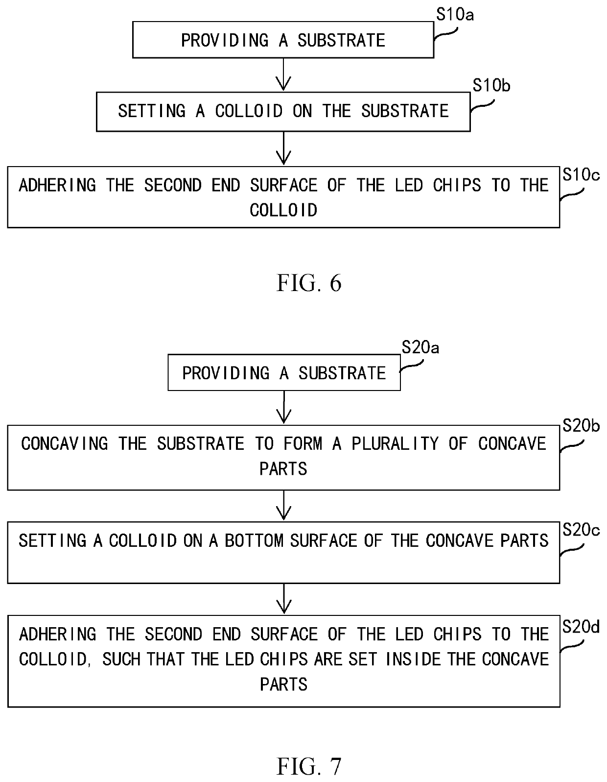
[0073]Specifically, the LED substrate 101 comprises a substrate 11, a colloid 12, and a plurality of LED chips 13.

[0074]Based on actual conditions of demand, the substrate 11 can be a hard substrate, for example, a glass substrate, and can also be a flexible substrate, for example, a polyimide substrate. In this first embodiment, the substrate 11 is a hard substrate, but it is not limited to that.

[0075]The colloid 12 is set on the substrate 11. The colloid 12 can be one of hot d...

second embodiment

[0090]The LED substrate 301 comprises an auxiliary layer 35. The auxiliary layer 35 is set on the substrate 31, and the auxiliary layer 35 comprises a plurality of through holes 351 that expose the substrate 31. The through holes and the exposed substrate 31 define the concave parts 34. Wherein, concerning the effect of setting the LED chip 33 inside the concave parts 34, please refer to the corresponding description in the

[0091]As a second end surface 332 of the LED chip 33 is a light outputting surface, the light outputting side of LED chip 33 is surrounded by the auxiliary layer 35. The auxiliary layer 35 improves interference between the lateral light of adjacent LED chips 33.

third embodiment

[0092]A material of the auxiliary layer 35 is a photoresist material, which can be one of polystyrene plastic, PFA (perfluoroalkoxy) plastic, or black resin material, but is not limited to that. In this third embodiment, the material of the auxiliary layer 35 is black resin photoresist, such that the auxiliary layer 35 can absorb the lateral light of the LED chips 33.

[0093]In some other embodiments, the material of the auxiliary layer 35 can be photoresist doped with light absorbing particles, such that the auxiliary layer 35 is capable of absorbing the lateral light of the LED chips 33. Furthermore, as the photoresist is doped with light absorbing particles, the wall of the through hole 351 is rough, which increases the stability of the colloid 12 and the auxiliary layer 35, thereby increasing the overall stability when the colloid 12 is in the final stage of curing.

[0094]Concerning the method for providing LED substrate in this third embodiment, please refer to the detail of the s...


PUM


Abstract

The present application provides an LED substrate and a method for manufacturing an LED display panel. The LED substrate comprises a substrate, a colloid, and LED chips. The colloid is set on the substrate, and the LED chips comprise a first end surface and a second end surface, wherein the first end surface and the second end surface are set opposite to each other, the first end surface is for fixedly connecting a thin film transistor substrate, and the second end surface is a light outputting surface. The second end surface of the LED chips is fixedly set on the substrate by the colloid.

Description

BACKGROUND OF INVENTIONField of Invention[0001]The present application relates to a display technology, and particularly to an LED substrate and a method for manufacturing an LED display panel.Description of Prior Art[0002]Currently, in the method for manufacturing a micro light-emitting diode (micro-LED) display panel, limited by influences of equipment precision and machine size, the manufacturing method is as follows: firstly, placing LEDs on a temporary substrate; secondly, grabbing the LEDs placed on the temporary substrate with a transferring device and jointing them with thin film transistor substrates to form small-sized display panels; and finally, splicing the small-sized display panels to form a large-sized display panel.[0003]For example, to form an 80 inch display panel, the present practice is jointing a 10-inch thin film transistor substrate with LEDs to form a 10-inch display panel and then integrating 8*8=64 pieces of small-sized display panels by splicing to achiev...

Claims


Application Information

Patent Timeline
IPC IPC(8): H01L25/075H01L27/12H01L33/62
CPCH01L25/0753H01L2933/0066H01L33/62H01L27/1214H01L33/48H01L21/50H01L25/167G09F9/33H01L2933/0033H01L2224/95
Inventor CHEN, SHUJHIH
Owner SHENZHEN CHINA STAR OPTOELECTRONICS SEMICON DISPLAY TECH CO LTD
Why Eureka
Try Eureka