
Packaging structure, manufacturing method of packaging structure, and quantum processor

Active Publication Date: 2021-11-18
ALIBABA GRP HLDG LTD
View PDF3 Cites 1 Cited by
  • Summary
  • Abstract
  • Description
  • Claims
  • Application Information

AI Technical Summary

Benefits of technology

The patent text describes a method of adding an air bridge to a coplanar waveguide to create a capacitor that can help reduce interference with existing resonance frequencies. This can help improve high-frequency signal transmission. By reducing the intensity of the induced electric field, the loss factor of a single air bridge can be minimized. The technical effect of this method is an improved performance of coplanar waveguides in high-frequency signal transmission.

Problems solved by technology

However, the introduction of air bridges increases energy loss, which can reduce the internal quality factor (Qi) value of the CPW, thereby affecting the performance of the entire packaging structure.
The air bridge developed by the hot-melt deformation of photoresist in processing and shaping can cause to leave a dielectric layer that is difficult to remove on the surface of the air bridge.
Therefore, the resulting dielectric loss of the processed air bridge can be high.
However, no known solutions have been found to reduce dielectric loss to reduce the impact on Qi.

Method used


Image

  • Packaging structure, manufacturing method of packaging structure, and quantum processor
  • Packaging structure, manufacturing method of packaging structure, and quantum processor
  • Packaging structure, manufacturing method of packaging structure, and quantum processor

Examples


Embodiment Construction

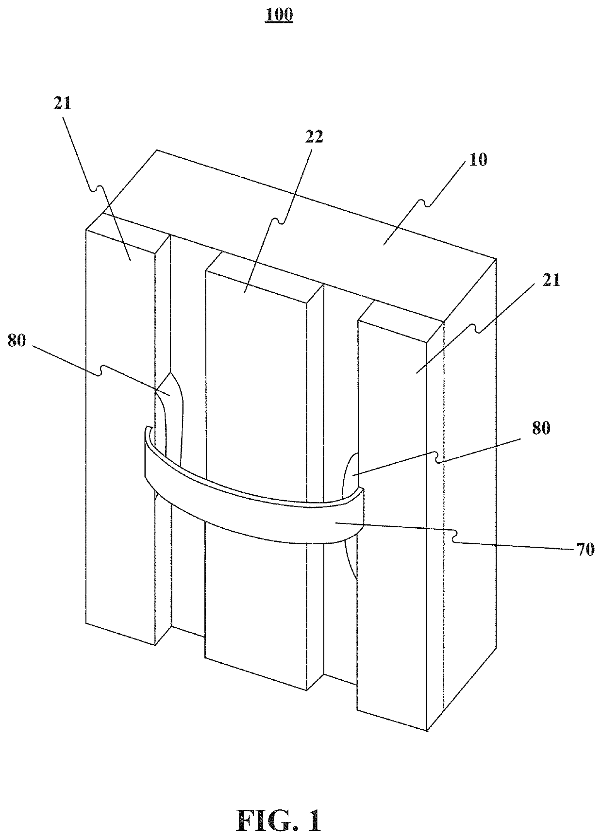
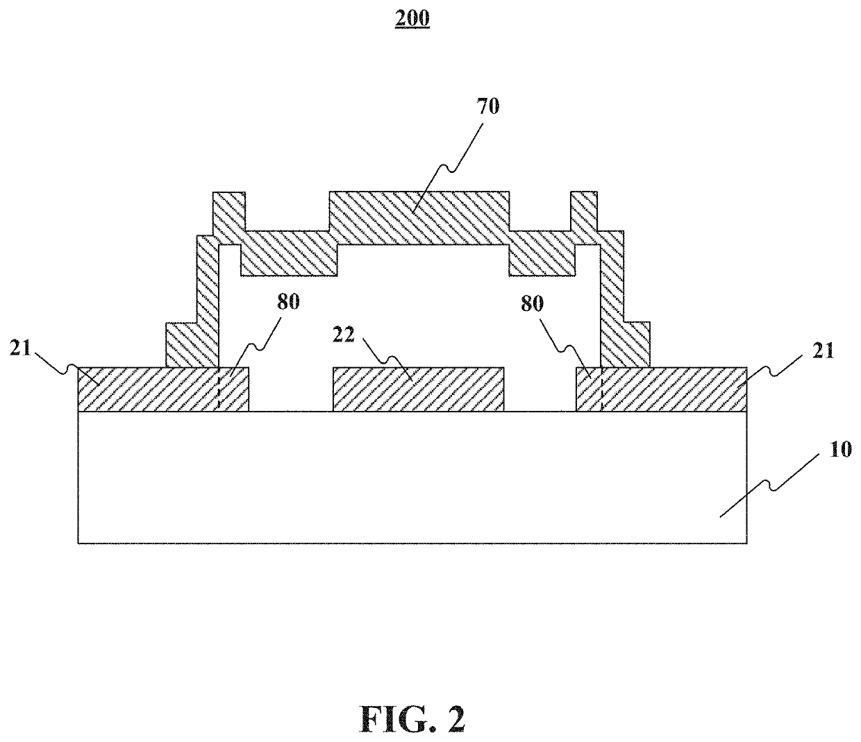
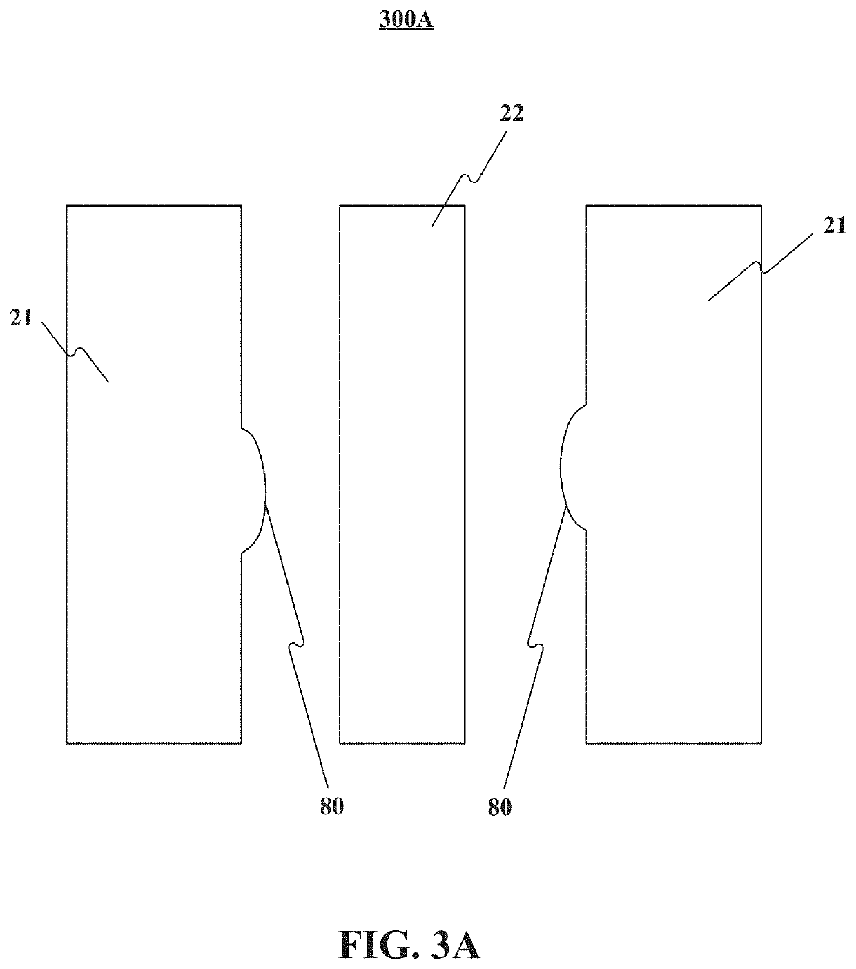
[0024]Technical solutions disclosed in the embodiments of the present disclosure can be described with reference to the accompanying drawings in the embodiments of the present disclosure. It is apparent that the described embodiments are merely some of, rather than all, the embodiments of the present disclosure. Based on the embodiments of the present disclosure, all other embodiments derived by those of ordinary skill in the art without creative efforts fall within the protection scope of the present disclosure.

[0025]The terms used in the embodiments of the present disclosure are for the purpose of describing particular embodiments only, and are not intended to limit the present disclosure. The singular forms “a,”“said,” and “the” used in the embodiments of the present disclosure and the appended claims are also intended to include plural forms, unless other meanings are clearly indicated in the context. “Plurality” includes at least two. In addition, references to “one embodiment”...


PUM


Abstract

A packaging structure, a method of manufacturing a packaging structure, and a quantum processor include a substrate; a coplanar waveguide including a first ground wire, a second ground wire, and a signal wire, wherein the first ground wire, the second ground wire, and the signal wire are disposed on a surface of the substrate at intervals, and the signal wire is located between the first ground wire and the second ground wire; an air bridge including a first end connected with the first ground wire and a second end connected with the second ground wire, wherein a gap exists between the air bridge and a surface of the signal wire away from the substrate; and a compensation structure located on the surface of the substrate.

Description

CROSS-REFERENCE TO RELATED APPLICATIONS[0001]This application claims priority to Chinese Application 202010403384.7, filed on May 13, 2020, the content of which is incorporated herein by reference in its entirety.TECHNICAL FIELD[0002]The present disclosure relates to the field of quantum chips, and in particular, to a packaging structure, a manufacturing method of a packaging structure, and a quantum processor.BACKGROUND[0003]In the field of superconducting quantum computing chips, three-dimensional (3D) integration based on an air bridge is a conventional solution for preparing a superconducting packaging structure. Typically, a suspended air bridge of an arched structure is processed at two ends of a coplanar waveguide (CPW) by a photoresist hot-melt method and a photoresist removal process so as to connect ground wires at the two ends, thereby realizing the 3D integration solution for the superconducting packaging structure. 3D integration based on an air bridge can enable develo...

Claims


Application Information

Patent Timeline
IPC IPC(8): H01P3/00H05K1/02
CPCH01P3/003H05K1/0237H01L23/535H01L21/76895H01P3/006G06N10/00H01P1/162H01P11/003
Inventor XU, HUAQIN, JIN
Owner ALIBABA GRP HLDG LTD
Learn More