Eureka AIR delivers breakthrough ideas for toughest innovation challenges, trusted by R&D personnel around the world.

Wafer level chip scale packaging with sensor

a chip scale and sensor technology, applied in the field of packaging including a sensor die and an integrated circuit die, can solve the problems of reducing the likelihood of failure in semiconductor device packaging, and achieve the effect of increasing the useful life and increasing the useful life of the embodiment of the present disclosur

Pending Publication Date: 2021-12-23
STMICROELECTRONICS PTE LTD
View PDF0 Cites 0 Cited by
  • Summary
  • Abstract
  • Description
  • Claims
  • Application Information

AI Technical Summary

Benefits of technology

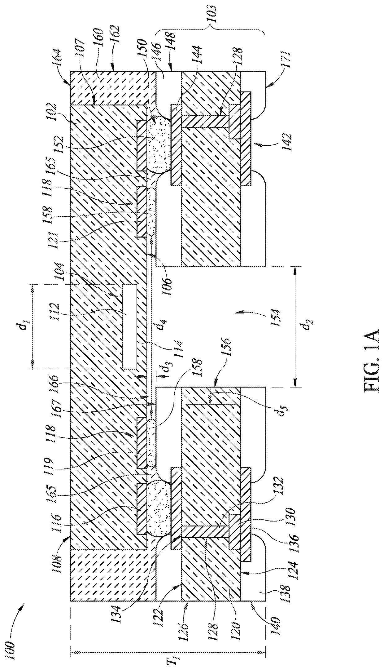
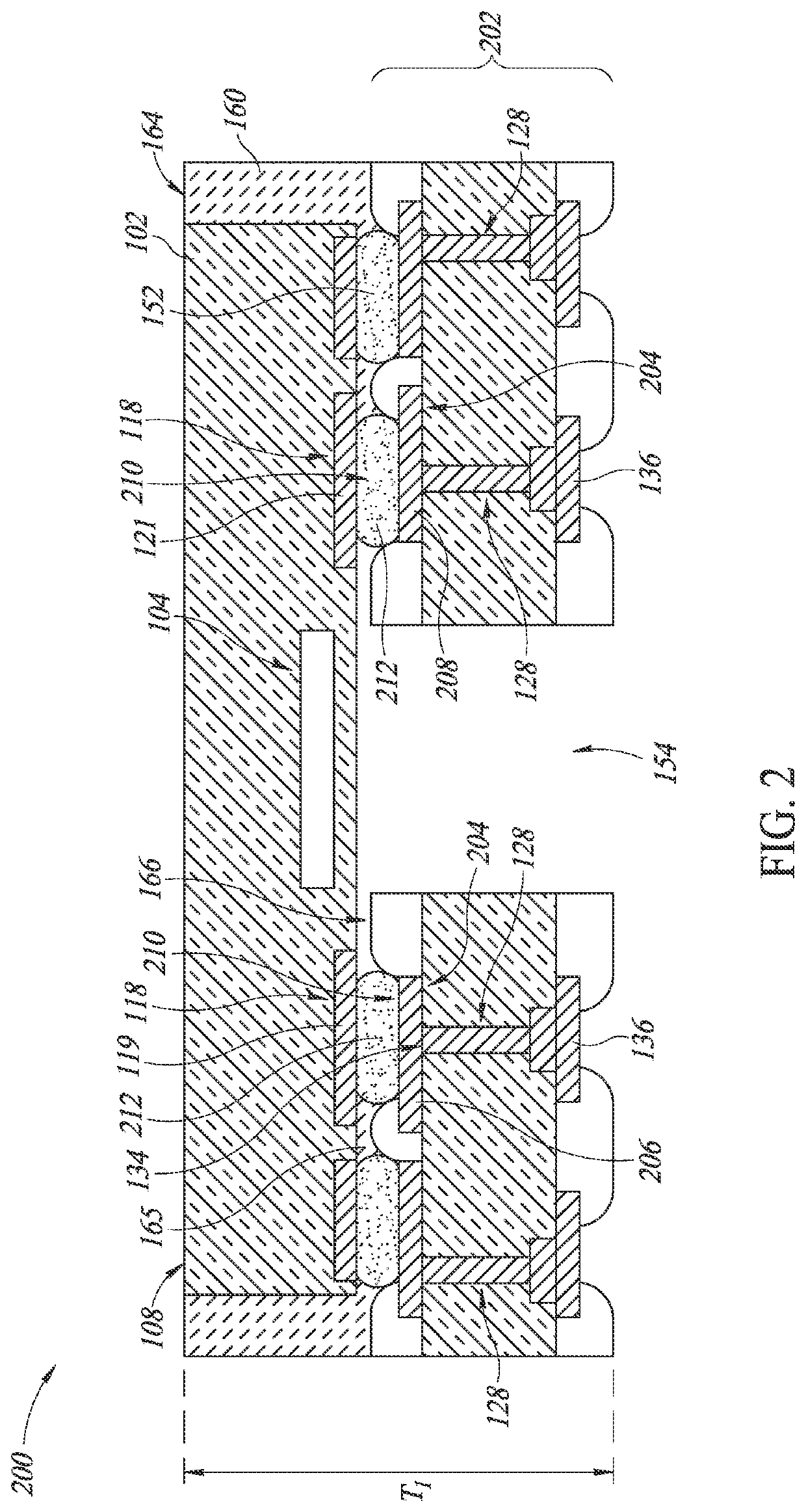
The present invention removes the cap requirement for semiconductor device packages, reducing the likelihood of failure due to temperature changes. The resulting package is smaller and thinner than conventional packages. Additionally, the useful lifespan of the semiconductor device packages is increased because of the lower likelihood of the components breaking off due to differences in expansion and contraction.

Problems solved by technology

One significant challenge is to reduce the likelihood of failure in semiconductor device packages when exposed to temperature changes due to differences in coefficients of thermal expansion (CTEs) of various materials of semiconductor device packages.

Method used


Image

  • Wafer level chip scale packaging with sensor
  • Wafer level chip scale packaging with sensor
  • Wafer level chip scale packaging with sensor

Examples


Embodiment Construction

[0023]In the following description, certain specific details are set forth in order to provide a thorough understanding of various embodiments of the disclosure. However, one skilled in the art will understand that the disclosure may be practiced without these specific details. In other instances, well-known structures associated with electronic components, packages, and semiconductor fabrication techniques have not been described in detail to avoid unnecessarily obscuring the descriptions of the embodiments of the present disclosure.

[0024]Unless the context requires otherwise, throughout the specification and claims that follow, the word “comprise” and variations thereof, such as “comprises” and “comprising,” are to be construed in an open, inclusive sense, that is, as “including, but not limited to.”

[0025]The use of ordinals such as first, second, third, etc., does not necessarily imply a ranked sense of order, but rather may only distinguish between multiple instances of an act o...


PUM

PropertyMeasurementUnit
conductiveaaaaaaaaaa
dimensionaaaaaaaaaa
non-conductiveaaaaaaaaaa

Abstract

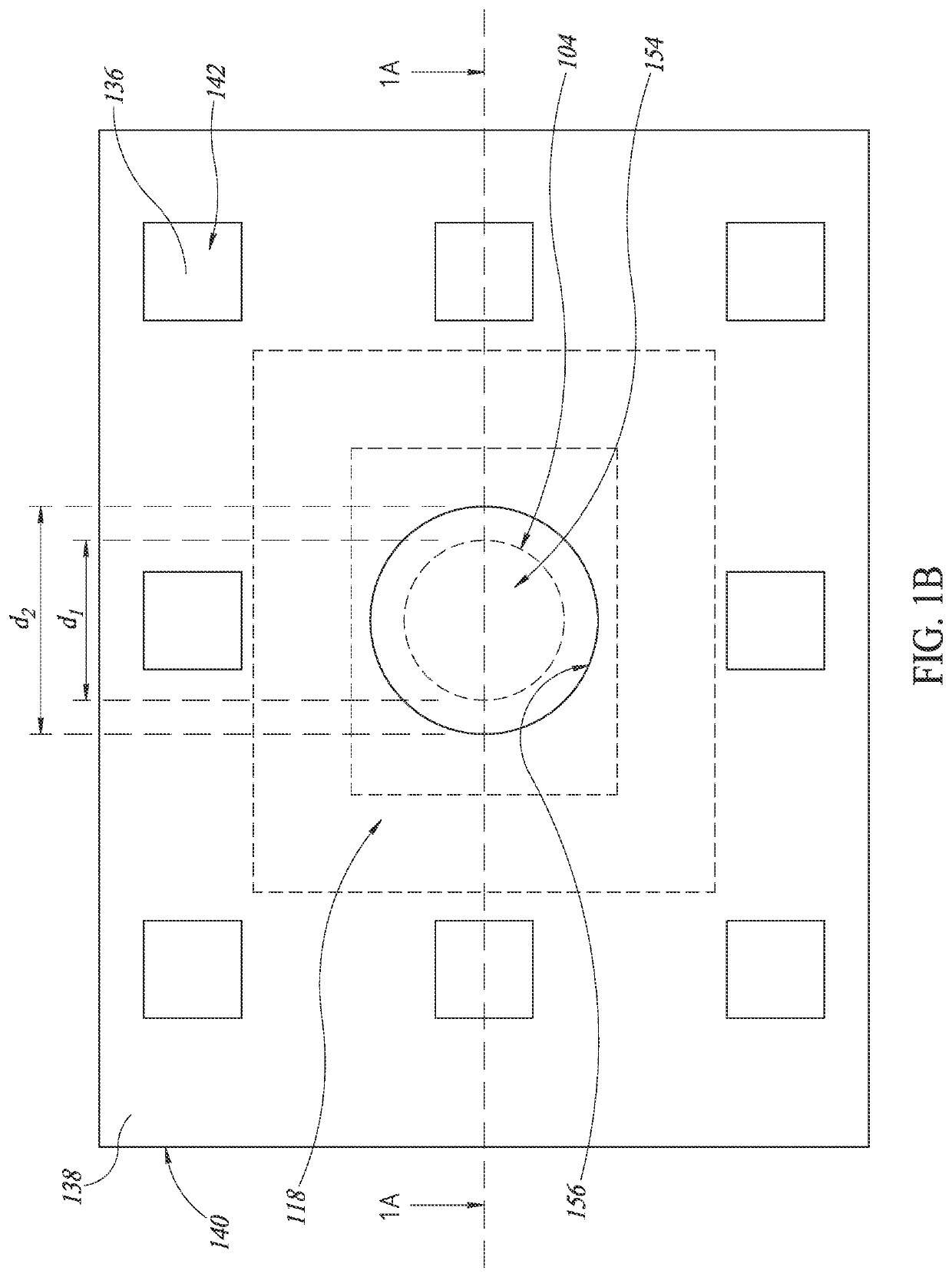
The present disclosure is directed to a package (e.g., a chip scale package, a wafer level chip scale package (WLCSP), or a package containing a sensor die) with a sensor die on a substrate (e.g., an application-specific integrated circuit die (ASIC), an integrated circuit, or some other type of die having active circuitry) and encased in a molding compound. The sensor die includes a sensing component that is aligned with a centrally located opening that extends through the substrate. The centrally located opening extends through the substrate at an inactive portion of the substrate. The centrally located opening exposes the sensing component of the sensor die to an external environment outside the package.

Description

BACKGROUNDTechnical Field[0001]The present disclosure is directed to a package including a sensor die and an integrated circuit die.Description of the Related Art[0002]Generally, semiconductor device packages, such as chip scale packages or wafer level chip scale packages (WLCSP), contain dice, such as sensors configured to detect any number of quantities or qualities of an external environment outside the packages. For example, semiconductor device packages may detect light, temperature, sound, pressure, vibration, or any other quantities or qualities of the external environment outside the packages.[0003]Stacking die on top of substrates, such as printed circuit boards (PCBs) or application-specific integrated circuit (ASIC) dies, results in relatively bulky packages. As demand increases for smaller packages while maintaining the functionality of the packages with cost-effective manufacturing, manufacturers are continually working on ways to reduce the size, profile, and thickness...

Claims


Application Information

Patent Timeline
Patent Type & Authority Applications(United States)
IPC IPC(8): B81B7/00B81C1/00
CPCB81B7/0061B81B2207/07B81B2201/0264B81C1/00309H01L23/3114H01L23/10H01L23/16H01L25/071H01L25/16
Inventor LUAN, JING-EN
Owner STMICROELECTRONICS PTE LTD
Why Eureka
Eureka Blog
Learn More