Electronic device and manufacturing method therefor

a manufacturing method and technology of an electronic device, applied in the direction of semiconductor devices, basic electric elements, electrical equipment, etc., can solve the problems of increasing the cost compared with the use of resin adhesives, peeling off the window member from the substrate, etc., and achieve the effect of improving the bonding strength between the base member and the cover member and increasing the cos

Pending Publication Date: 2021-12-23
MURATA MFG CO LTD
View PDF0 Cites 0 Cited by
  • Summary
  • Abstract
  • Description
  • Claims
  • Application Information

AI Technical Summary

Benefits of technology

The present patent aims to provide an electronic device and a manufacturing method that can improve the strength of the bonding between a base member and a cover member without increasing cost. This will provide better durability and reliability for the electronic device.

Problems solved by technology

The bonding strength of ceramic materials such as LTCC and AlN with resin adhesives is comparatively weak, and therefore there is a problem in that there is a tendency for the window member to peel off from the substrate when a resin adhesive is used to bond the substrate and the window member to each other.
On the other hand, when the substrate and the window member are bonded to each other using gold-tin (AuSn) for example, there is an increase in cost compared with when a resin adhesive is used.

Method used


Image

  • Electronic device and manufacturing method therefor
  • Electronic device and manufacturing method therefor
  • Electronic device and manufacturing method therefor

Examples


Embodiment Construction

[0016]Hereafter, an embodiment of the present disclosure will be described. In the following description of the drawings, identical or similar constituent elements are denoted by identical or similar reference symbols. The drawings are representative, the dimensions and shapes of the individual parts are schematically illustrated, and the technical scope of the invention of the present application should not be interpreted as being limited to that of the embodiment.

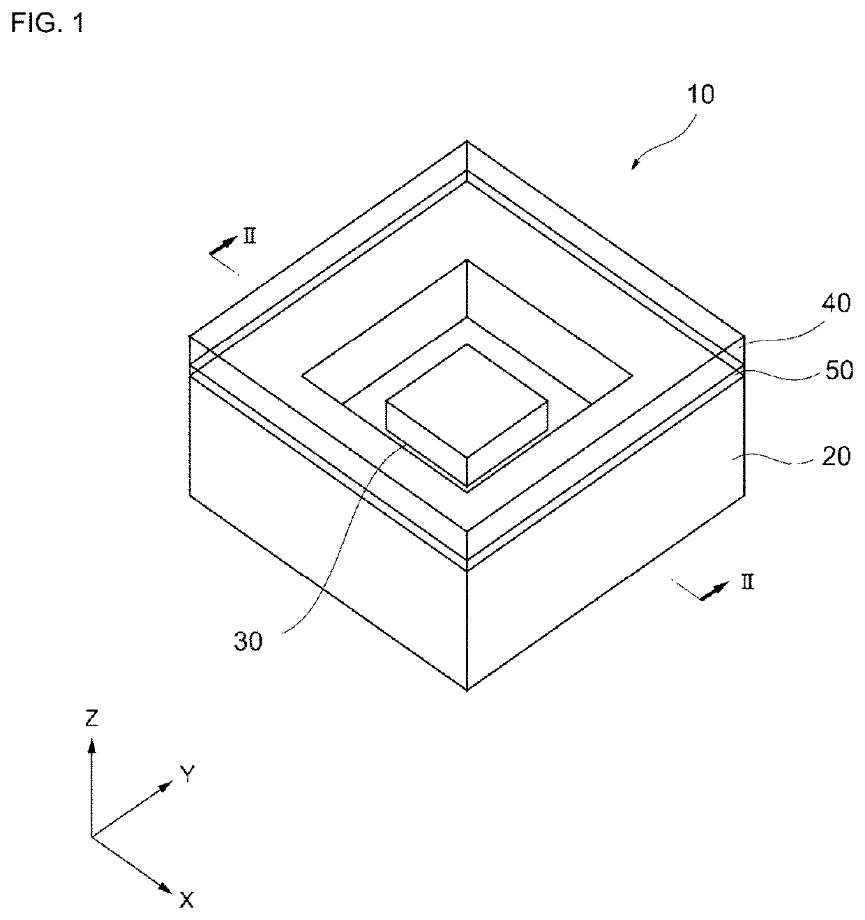
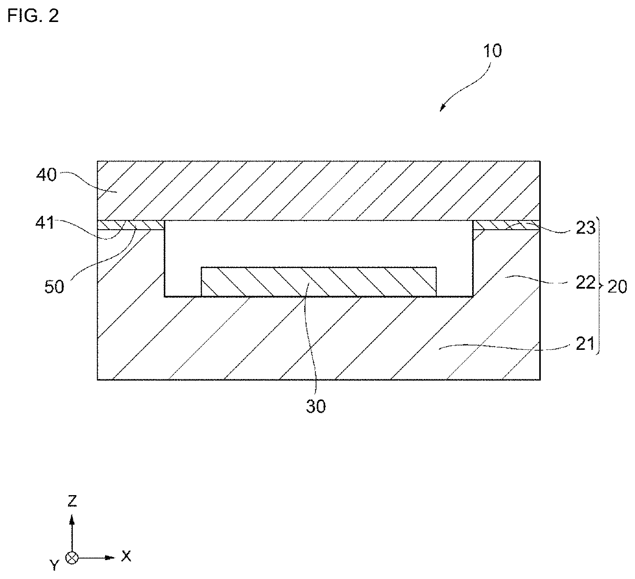
[0017]A light-emitting device according to an embodiment of the present disclosure will be described while referring to FIGS. 1 and 2. FIG. 1 is a perspective view of the light-emitting device according to the embodiment of the present disclosure. FIG. 2 is a sectional view taken along line II-II in FIG. 1.

[0018]As illustrated in FIG. 1, a light-emitting device 10 according to this embodiment includes a base member 20, a light-emitting element 30, a cover member 40, and an organic structure 50. Hereafter, for convenience ...


PUM

PropertyMeasurementUnit
wavelength regionaaaaaaaaaa
organicaaaaaaaaaa
surface roughnessaaaaaaaaaa

Abstract

An electronic device that includes a base member made of a material containing metal atoms, the base member having a bonding surface, and the bonding surface contains oxides of the metal atoms; an electronic element is mounted on the base member; an organic structure on the bonding surface of the base member; and a cover member bonded to the bonding surface of the base member via the organic structure so as to encapsulate the electronic element in a space between the base member and the cover member.

Description

CROSS REFERENCE TO RELATED APPLICATIONS[0001]The present application is a continuation of International application No. PCT / JP2020 / 000839, filed Jan. 14, 2020, which claims priority to Japanese Patent Application No. 2019-101308, filed May 30, 2019, the entire contents of each of which are incorporated herein by reference.FIELD OF THE INVENTION[0002]The present disclosure relates to an electronic device and a manufacturing method therefor.BACKGROUND OF THE INVENTION[0003]Heretofore, a package structure in which an electronic element such as a light-emitting diode (LED) is encapsulated by a substrate and cover member is known. For example, below-listed Patent Document 1 discloses an ultraviolet light-emitting device in which a deep ultraviolet LED element is mounted inside a recess provided in a low-temperature co-fired ceramic (LTCC) substrate and the LTCC substrate and an ultraviolet light passing window member are bonded to each other by a resin adhesive layer. It is described in ...

Claims


Application Information

Patent Timeline
Patent Type & Authority Applications(United States)
IPC IPC(8): H01L33/48
CPCH01L33/483H01L2933/0033H01L33/48H01L33/58H01L2933/0058H01L33/54H01L2933/005
Inventor YOSHII, KENTAROMATSUSHITA, KOJI
Owner MURATA MFG CO LTD
Why Eureka
Try Eureka