Ligands for quantum dots in cross-linked emissive layer of quantum dot light emitting diodes

a technology of light-emitting diodes and ligands, which is applied in the field of light-emitting devices, can solve the problems of higher fabrication cost and complexity, and achieve the effects of improving the performance of existing qleds, improving the patterned layer, and improving the structure of a layer

Active Publication Date: 2021-12-30
SHARP KK
View PDF0 Cites 4 Cited by
  • Summary
  • Abstract
  • Description
  • Claims
  • Application Information

AI Technical Summary

Benefits of technology

[0006]The present application relates to an enhanced structure of a layer including Quantum Dots (QDs) dispersed in a cross-linked material. A layer including QDs dispersed in a cross-linked material is resistant to solvent rinsing and may improve patterned layers in the QLED field. This can be generally called a cross-linked layer in which quantum dots are dispersed (CLQDL). In some embodiments, the quantum dots are dispersed in, but do not form a part of, the cross-linked network of the cross-linked layer. In other embodiments, the quantum dots are dispersed in, and form a part of, the cross-linked network of the cross-linked layer. In embodiments where the cross-linked material is a charge transport material (e.g., hole transport material or electron transport material), this layer may also be referred to as a combined charge transport and emissive layer (CCTEL) of a QLED. The CCTEL may improve performance of existing QLEDs and may simplify fabrication by combining properties of a charge transport layer and an emissive layer.

Problems solved by technology

Thermal evaporation methods are widely used for OLEDs, but they are more complex and have higher costs of fabrication as compared to solution process methods.

Method used


Image

  • Ligands for quantum dots in cross-linked emissive layer of quantum dot light emitting diodes
  • Ligands for quantum dots in cross-linked emissive layer of quantum dot light emitting diodes
  • Ligands for quantum dots in cross-linked emissive layer of quantum dot light emitting diodes

Examples


Embodiment Construction

[0042]Embodiments of the present invention will now be described with reference to the drawings, wherein like reference numerals are used to refer to like elements throughout. It will be understood that the figures are not necessarily to scale.

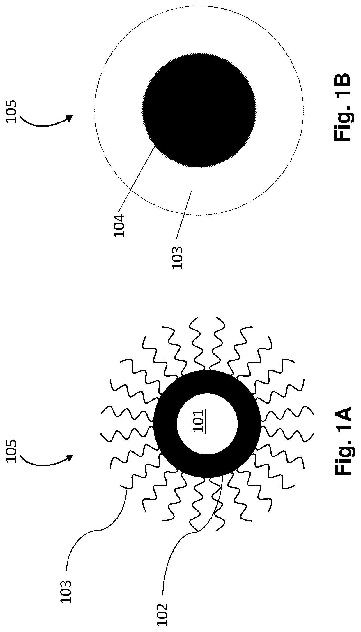
[0043]FIG. 1A and FIG. 1B are drawings depicting a two-dimensional schematic representation of a core-shell QD 105. Multiple instances of the QD 105 may be employed in an emissive layer. The QDs may be configured as nanoparticles. FIG. 1A schematically shows that the QD may include a nanocrystalline core 101 that is co-crystallized with a shell 102 including a compatible material, which is then surrounded by ligands103 (bonded / attached to the surface of the QD) that passivate crystal defects in the core-shell QD, i.e., core 101 and shell 102, and allow and improve solubility in common solvents. FIG. 1B is a schematic simplified version of FIG. 1A used for more convenient representation of QDs in a light-emitting device structure, depicting a g...


PUM

PropertyMeasurementUnit
charge transportaaaaaaaaaa
thicknessaaaaaaaaaa
thicknessaaaaaaaaaa

Abstract

A light-emitting device includes an anode, a cathode, and a crosslinked emissive layer disposed between the anode and the cathode in which quantum dots are dispersed. The crosslinked layer includes a crosslinked material and quantum dots dispersed in the crosslinked mater, the quantum dots having ligands respectively bonded to the quantum dots. The quantum dots are distributed unevenly within the crosslinked material. The ligands have a concentration relative to the weight of the quantum dots of 10 to 45 wt %. A method of forming a crosslinked emissive layer of a light-emitting device in which quantum dots are dispersed includes the steps of depositing a mixture on a deposition surface and subjecting at least a portion of the mixture to an activation stimulus to crosslink the cross-linkable material.

Description

TECHNICAL FIELD[0001]The present application relates to light-emitting devices, and in particular to light-emitting devices including a crosslinked emissive layer containing quantum dots. The light-emitting devices may be implemented in display applications, for example in high resolution, multicolor displays. The present application further relates to methods of fabricating such light-emitting devices.BACKGROUND ART[0002]A common architecture for a light-emitting device includes an anode, which acts as hole injector; a hole transport layer disposed on the anode; an emissive material layer disposed on the hole transport layer; an electron transport layer disposed on the emissive material layer; and a cathode, which also acts as an electron injector, disposed on the electron transport layer. When a forward bias is applied between the anode and cathode, holes and electrons are transported in the device through the hole transport layer and electron transport layer, respectively. The ho...

Claims


Application Information

Patent Timeline
Patent Type & Authority Applications(United States)
IPC IPC(8): H01L51/50H01L51/56C09K11/02
CPCH01L51/502H01L51/56H01L51/5072B82Y20/00C09K11/025H01L2251/56H01L51/5056H10K59/35H10K50/115H10K50/16H10K50/15H10K2101/80H10K71/00
Inventor ANGIONI, ENRICODE LA CALLE, ISABEL ARRANZSMEETON, TIM MICHAEL
Owner SHARP KK
Why Eureka
Try Eureka