Method of forming a conductive barrier layer having improved adhesion and resitivity characteristics

a technology of conductive barrier layer and resitivity, which is applied in the manufacture of basic electric elements, electrical equipment, semiconductor/solid-state devices, etc., can solve the problems of not being able to effectively patterned by anisotropic etching procedures, copper also exhibits, and cannot be efficiently applied to a substrate in large amounts. achieve the effect of improving adhesion characteristics

Inactive Publication Date: 2005-01-11
ADVANCED MICRO DEVICES INC
View PDF20 Cites 11 Cited by
  • Summary
  • Abstract
  • Description
  • Claims
  • Application Information

AI Technical Summary

Benefits of technology

Generally, the present invention is directed to an improved barrier layer technique in which substantially all of the interfaces of a metal interconnection to the surrounding materials have improved adhesion characteristics. In particular, at the bottom surfaces of damascene metallization structures, the deposition characteristics in manufacturing the barrier layer are controlled in such a manner that an improved barrier layer structure having the required adhesion qualities is obtained. To this end, process parameters during the sputter deposition of the barrier material are controlled to deposit a first component preferentially at the bottom surface without unduly contaminating the sidewall areas.

Problems solved by technology

Due to the large number of circuit elements and the required complex layout of the integrated circuits, generally the electrical connection of the individual circuit elements may not be established within the same level on which the circuit elements are manufactured, but requires one or more additional “wiring” layers, also referred to as metallization layers.
Since the fabrication of a plurality of metallization layers entails extremely challenging issues to be solved, such as mechanical, thermal and electrical reliability of up to twelve stacked metallization layers that are required, for example, for sophisticated aluminum-based microprocessors, semiconductor manufacturers are increasingly replacing the well-known metallization metal aluminum by a metal that allows higher current densities and hence allows reduction of the dimensions of the interconnections.
In spite of these advantages, copper also exhibits a number of disadvantages regarding the processing and handling of copper in a semiconductor facility.
For instance, copper may not be efficiently applied onto a substrate in larger amounts by well-established deposition methods, such as chemical vapor deposition (CVD), and also may not be effectively patterned by the usually employed anisotropic etch procedures.
A further major drawback of copper is its property to readily diffuse in silicon dioxide, which is a well-established and approved dielectric material in fabricating integrated circuits.
It turns out, however, that a single material may not readily meet the requirements imposed on a desired barrier material.
Tantalum, which effectively blocks copper atoms from diffusing into an adjacent material even when provided in extremely thin layers, however, exhibits only a poor adhesion to silicon dioxide based dielectrics, so that a copper interconnection including a tantalum barrier layer may suffer from reduced mechanical stability especially during the chemical mechanical polishing of the metallization layer, which is required for removing excess copper and planarizing the surface for the provision of a further metallization layer.
The reduced mechanical stability during the CMP may, however, entail severe reliability concerns in view of reduced thermal and electrical conductivity of the interconnections.
On the other hand, tantalum nitride exhibits excellent adhesion to silicon dioxide based dielectrics, but has very poor adhesion to copper.
The reduced adhesion of the barrier layer 110 on the copper 103 may lead to a significantly increased transition resistance due to partial delamination or due to a void formation at the interface 114, thereby significantly negatively affecting the device's reliability and performance.

Method used


Image

  • Method of forming a conductive barrier layer having improved adhesion and resitivity characteristics
  • Method of forming a conductive barrier layer having improved adhesion and resitivity characteristics
  • Method of forming a conductive barrier layer having improved adhesion and resitivity characteristics

Examples


Embodiment Construction

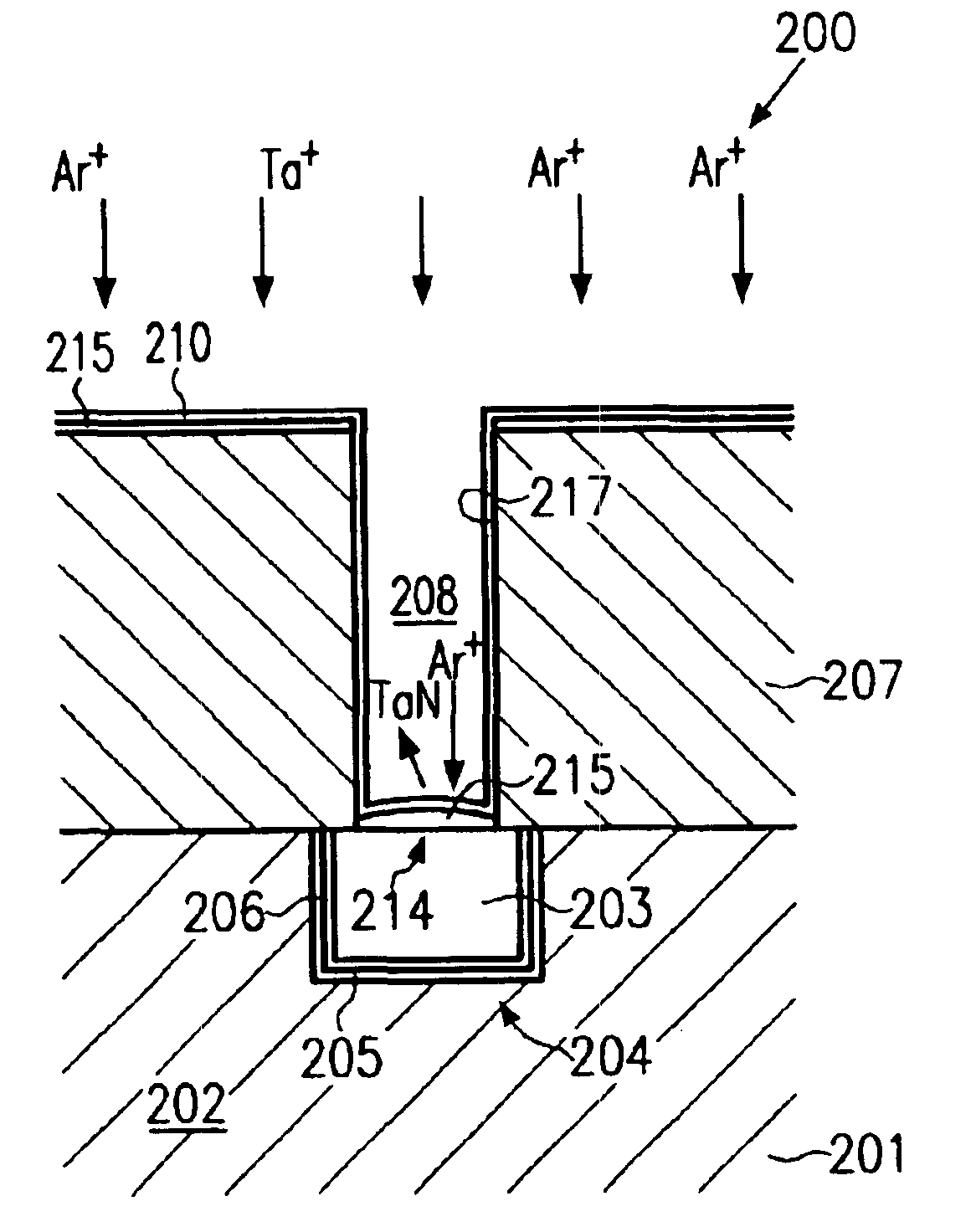
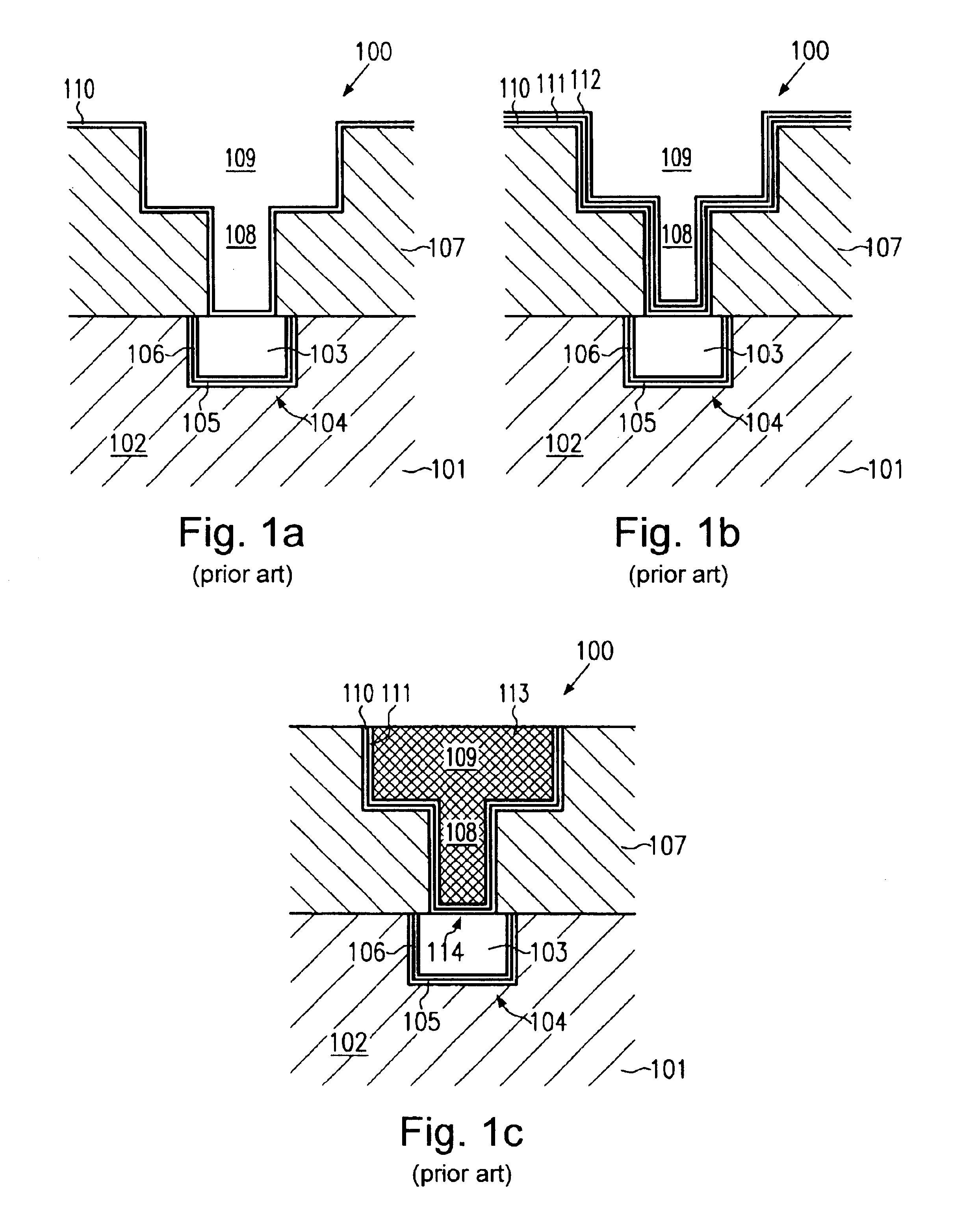
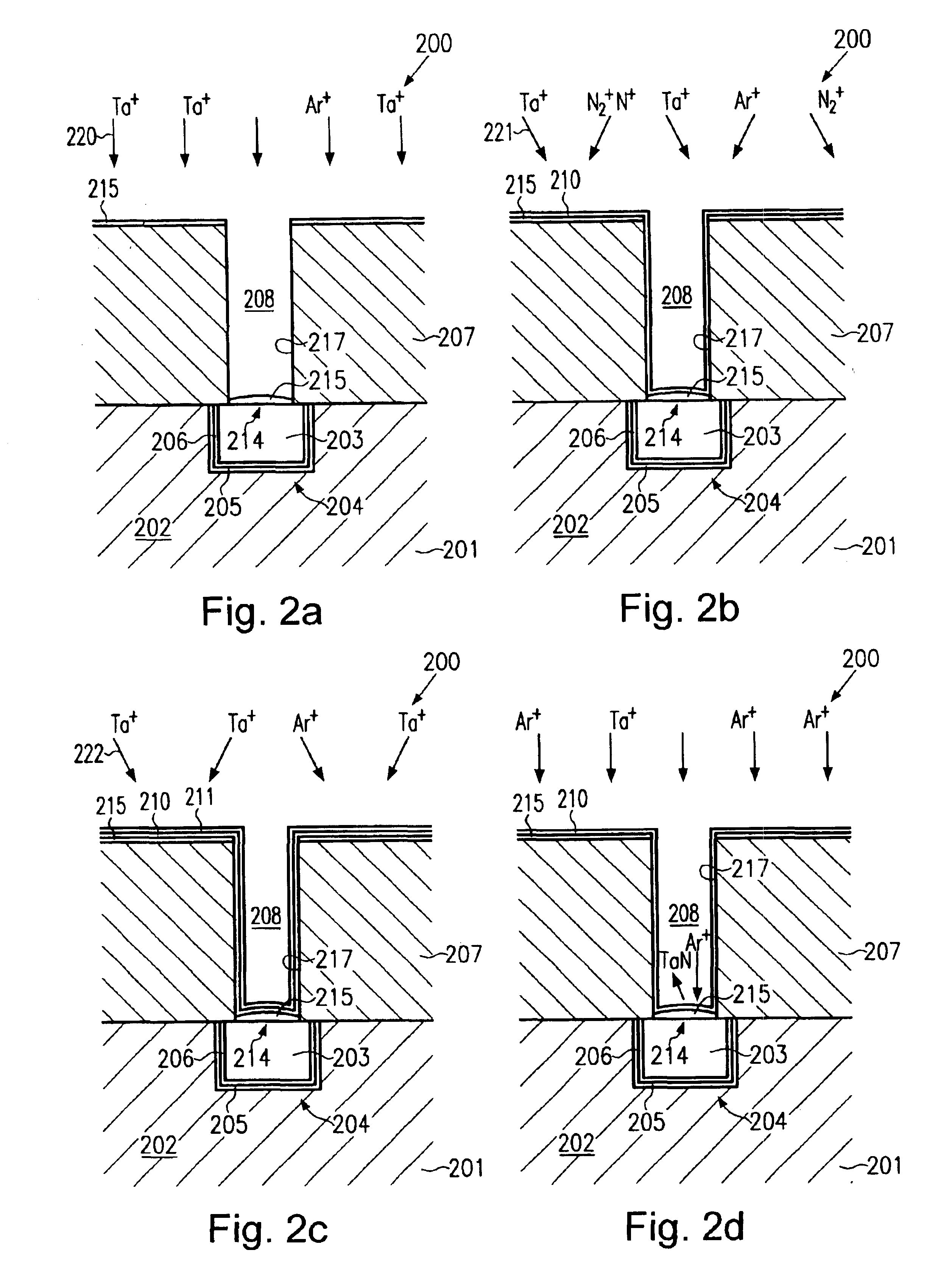
Illustrative embodiments of the invention are described below. In the interest of clarity, not all features of an actual implementation are described in this specification. It will of course be appreciated that in the development of any such actual embodiment, numerous implementation-specific decisions must be made to achieve the developers' specific goals, such as compliance with system-related and business-related constraints, which will vary from one implementation to another. Moreover, it will be appreciated that such a development effort might be complex and time-consuming, but would nevertheless be a routine undertaking for those of ordinary skill in the art having the benefit of this disclosure.

The present invention will now be described with reference to the attached figures. Although the various regions and structures of a semiconductor device are depicted in the drawings as having very precise, sharp configurations and profiles, those skilled in the art recognize that, in ...


PUM

PropertyMeasurementUnit
thicknessaaaaaaaaaa
thicknessaaaaaaaaaa
thicknessaaaaaaaaaa

Abstract

The adhesion properties of a metal interconnect structure are enhanced by selectively depositing a barrier layer component having good adhesion to an underlying metal on the bottom surface of a via. Then, a further barrier layer having superior adhesion characteristics for the dielectric is formed on the dielectric sidewalls of the via, so that excellent adhesion to the dielectric and the underlying metal is achieved. The selectivity of the deposition may be accomplished by exploiting the capabilities of modem IPVD tools.

Description

BACKGROUND OF THE INVENTION1. Field of the InventionThe present invention generally relates to the field of fabrication of integrated circuits, and, more particularly, to the formation of an interconnection requiring the provision of a barrier layer between a bulk metal and a dielectric in which the interconnection is embedded.2. Description of the Related ArtIn an integrated circuit, a huge number of circuit elements, such as transistors, capacitors, resistors, and the like, are formed in or on an appropriate substrate, usually in a substantially planar configuration. Due to the large number of circuit elements and the required complex layout of the integrated circuits, generally the electrical connection of the individual circuit elements may not be established within the same level on which the circuit elements are manufactured, but requires one or more additional “wiring” layers, also referred to as metallization layers. These metallization layers generally include metal lines, ...

Claims


Application Information

Patent Timeline
Patent Type & Authority Patents(United States)
IPC IPC(8): H01L21/02H01L21/285H01L21/70H01L21/768
CPCH01L21/2855H01L21/76843H01L21/76865H01L21/76862H01L21/76849
Inventor FRIEDEMANN, MICHAELKAHLERT, VOLKER
Owner ADVANCED MICRO DEVICES INC
Why Eureka
Try Eureka