QLED fabricated by patterning with phase separated emissive layer

a phase separated emissive layer and patterning technology, applied in the direction of basic electric elements, semiconductor devices, electrical apparatus, etc., can solve the problems of high fabrication cost, limited applicability to useful applications, and complex structure of qd-led layer, and achieves improved emissive layer structure, easy fabrication, and small size

Active Publication Date: 2020-11-03
SHARP KK
View PDF4 Cites 5 Cited by
  • Summary
  • Abstract
  • Description
  • Claims
  • Application Information

AI Technical Summary

Benefits of technology

[0008]The present application describes an enhanced QD-LED layer structure and related methods of fabricating such a structure that achieve optimal distribution of the quantum dots within the emissive layer for peak efficiency for the emission of light. In contrast to conventional configurations, a light-emitting device fabricated in accordance with embodiments of the present application includes a combined charge transport and emissive layer (CCTEL), which combines properties of a charge transport layer and an emissive layer. By using a CCTEL, additional charge transport layers may be rendered superfluous, which results in a structure that is smaller in size, easier to fabricate, and includes fewer deficiencies caused by interactions at layer interfaces.

Problems solved by technology

Thermal evaporation methods are widely used for OLEDs, but they are more complex and have higher costs of fabrication as compared to solution process methods.
The Coe-Sullivan structures are shown only with Cd-based, Pb-based and Gold QDs, and thus are of limited applicability to useful applications.
Even with such processes, issues remain as to how to fabricate and deposit the various device layers in a manner that achieves optimal distribution of the quantum dots within the emissive layer for peak light emission efficiency.

Method used


Image

  • QLED fabricated by patterning with phase separated emissive layer
  • QLED fabricated by patterning with phase separated emissive layer
  • QLED fabricated by patterning with phase separated emissive layer

Examples


Embodiment Construction

[0020]Embodiments of the present invention will now be described with reference to the drawings, wherein like reference numerals are used to refer to like elements throughout. It will be understood that the figures are not necessarily to scale.

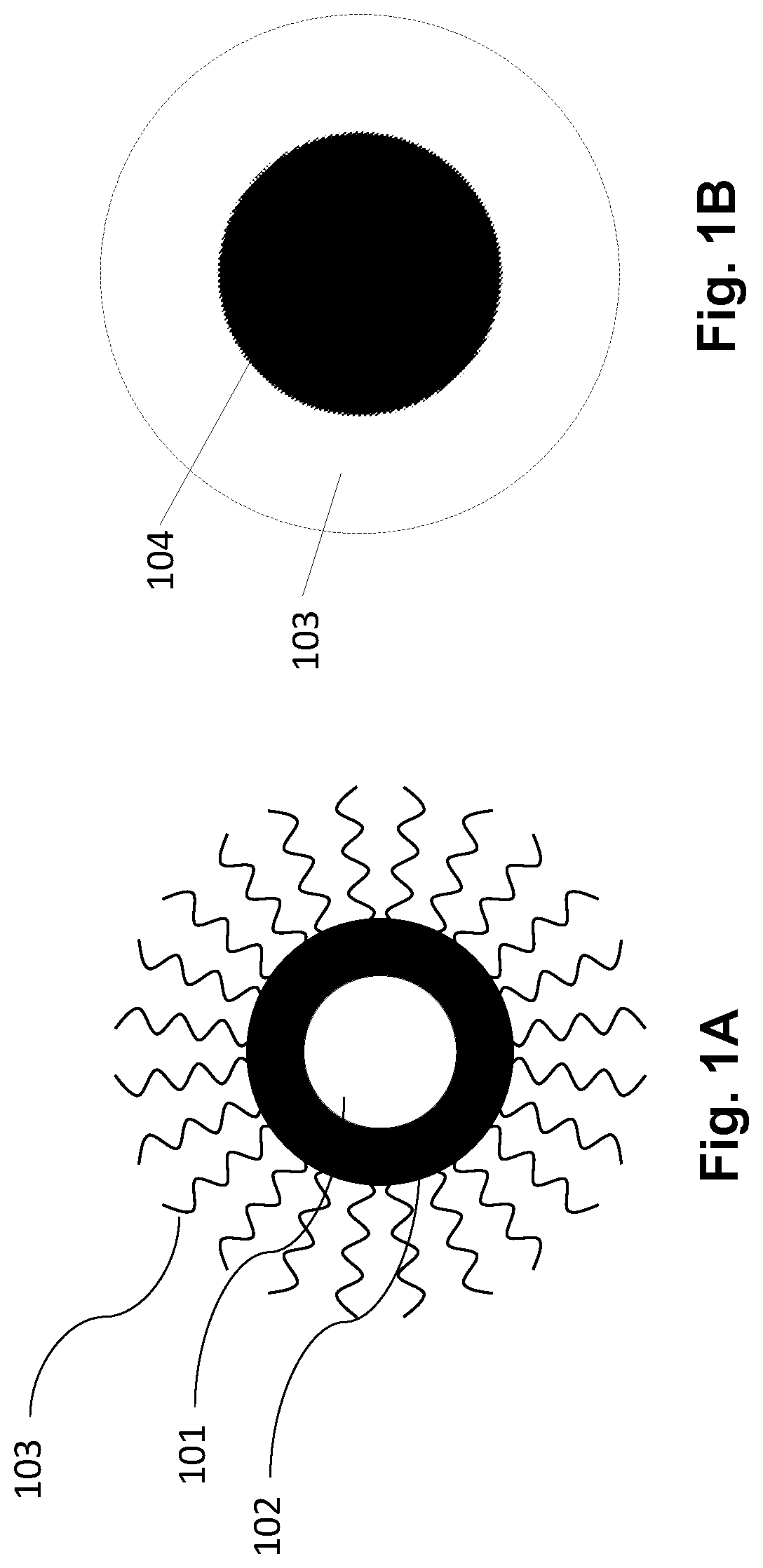
[0021]FIG. 1A and FIG. 1B are drawings depicting a two-dimensional schematic representation of a conventional core-shell QD as may be employed in a conventional emissive layer. The quantum dots may be configured as nanoparticles. A nanocrystalline core 101 is co-crystallised with a shell of a compatible material 102, which is then surrounded by ligands 103 that passivate crystal defects in the core-shell QD and allow and improve solubility in common solvents. FIG. 1B is a schematic simplified version of FIG. 1A used for more convenient representation of QDs in a light-emitting device structure, depicting a generalized core-shell QD structure 104 surrounded by a region of ligands 103.

[0022]Exemplary quantum dot core and shell materials include ...


PUM

PropertyMeasurementUnit
charge transportaaaaaaaaaa
distanceaaaaaaaaaa
areaaaaaaaaaaa

Abstract

A light-emitting device includes a combined charge transport and emissive layer (CCTEL). The light-emitting device includes an anode, a cathode, and a CCTEL disposed between the anode and the cathode, the CCTEL comprising a crosslinked charge transport material and quantum dots. The quantum dots are distributed unevenly within the crosslinked charge transport material. The quantum dots may be phase separated from the crosslinked charge transport material whereby the quantum dots form a layer at least partially within the CCTEL at or adjacent to an outer surface of the CCTEL closest to the cathode or the anode. The quantum dots may phase separate from the crosslinked material at least in part during the deposition of a mixture including the crosslinked material and quantum dots in a solvent, as the solvent component of the mixture evaporates. The quantum dots may phase separate from the crosslinked material at least in part in response to an activation stimulus, such as exposure to UV light.

Description

TECHNICAL FIELD[0001]The present application relates to light-emitting devices, and in particular to light-emitting devices including a crosslinked emissive layer containing nanoparticles. The light-emitting devices may be implemented in display applications, for example in high resolution, multicolor displays. The present application further relates to methods of fabricating such light-emitting devices.BACKGROUND ART[0002]A common architecture for a light-emitting device includes an anode, which acts as hole injector; a hole transport layer disposed on the anode; an emissive material layer disposed on the hole transport layer; an electron transport layer disposed on the emissive material layer; and a cathode, which also acts as an electron injector, disposed on the electron transport layer. When a forward bias is applied between the anode and cathode, holes and electrons are transported in the device through the hole transport layer and electron transport layer, respectively. The h...

Claims


Application Information

Patent Timeline
Patent Type & Authority Patents(United States)
IPC IPC(8): H01L51/50H01L27/32H01L51/00H01L51/56
CPCH01L51/5056H01L51/0007H01L51/502H01L51/5072H01L27/3246H01L51/56H01L51/0065H01L51/0061H01L51/0058H01L51/006H10K59/30H10K50/115H10K50/15H10K50/16H10K50/80H10K71/00H10K85/111H10K85/115H10K50/852H10K2102/321H10K59/122H10K71/15H10K85/626H10K85/633H10K85/636H10K85/653
Inventor ANGIONI, ENRICOSMEETON, TIM MICHAEL
Owner SHARP KK
Why Eureka
Try Eureka