Organic light-emitting diode display device

a light-emitting diode and display device technology, applied in the direction of diodes, semiconductor devices, electrical appliances, etc., can solve the problems of eye fatigue, decreased and worse visibility of users, so as to reduce the luminance of light emitted from organic light-emitting diodes. , the effect of increasing the overall luminance of organic light-emitting diodes

Pending Publication Date: 2022-01-20
LG DISPLAY CO LTD
View PDF0 Cites 0 Cited by
  • Summary
  • Abstract
  • Description
  • Claims
  • Application Information

AI Technical Summary

Benefits of technology

[0007]The inventors of the present disclosure have recognized such approach in the related art of disposing the circular polarizer on the upper surface of the display panel causes a problem of decreasing the overall luminance of the organic light-emitting diode display device. That is, since the transmittance of the circular polarizer is about 40%-50%, the luminance of the light emitted from the light-emitting diode is decreased by about 50% or more while passing through the circular polarizer.

Problems solved by technology

The inventors of the present disclosure have recognized such approach in the related art of disposing the circular polarizer on the upper surface of the display panel causes a problem of decreasing the overall luminance of the organic light-emitting diode display device.
However, the inventors of the present disclosure have appreciated that the antireflection film may generate a rainbow phenomenon and the rainbow phenomenon may worsen the visibility and may cause eye fatigue of the user.
Accordingly, the external light reflectance increases at the side view, and the visibility in the off state, that is, the black visibility can deteriorate, thereby causing a problem of decreasing the outdoor visibility and lowering the contrast ratio.

Method used


Image

  • Organic light-emitting diode display device
  • Organic light-emitting diode display device
  • Organic light-emitting diode display device

Examples


first embodiment

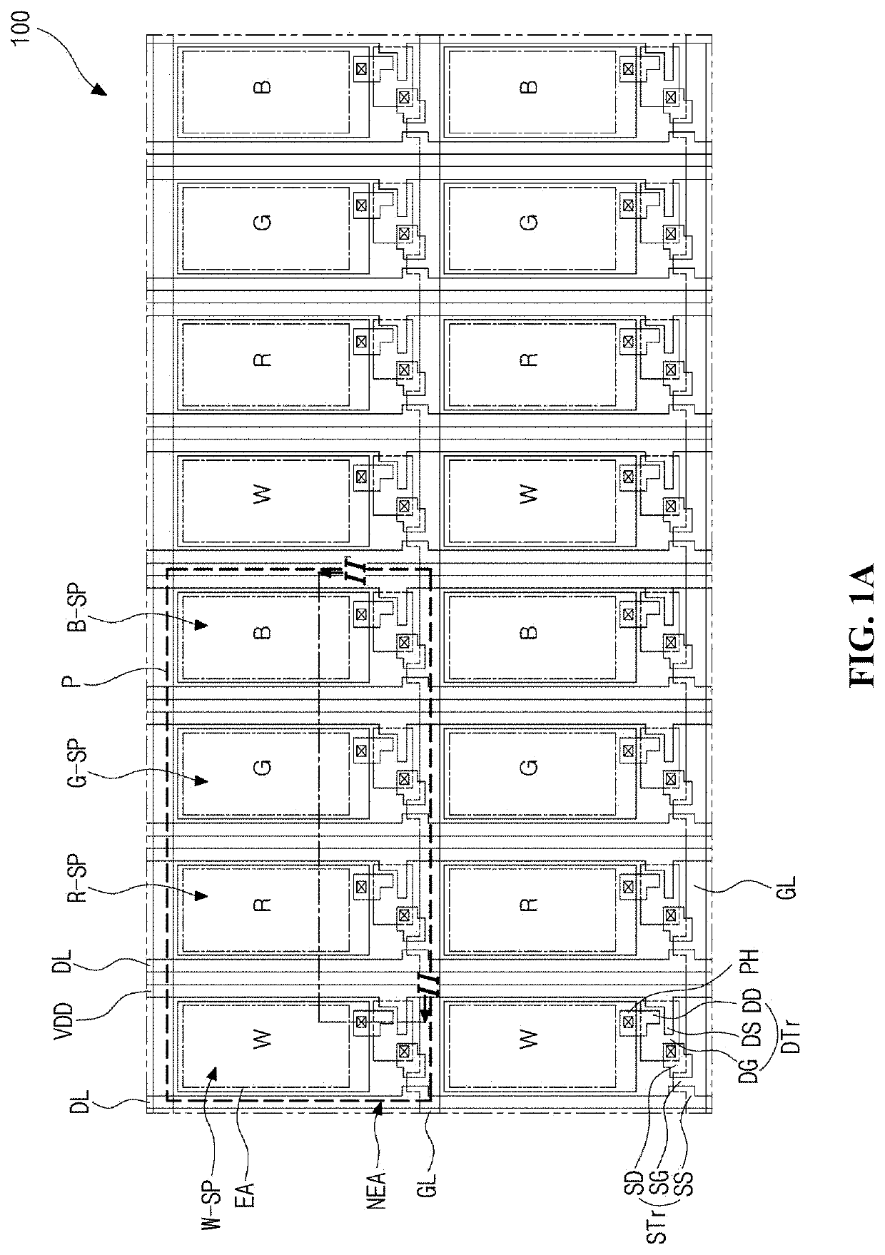
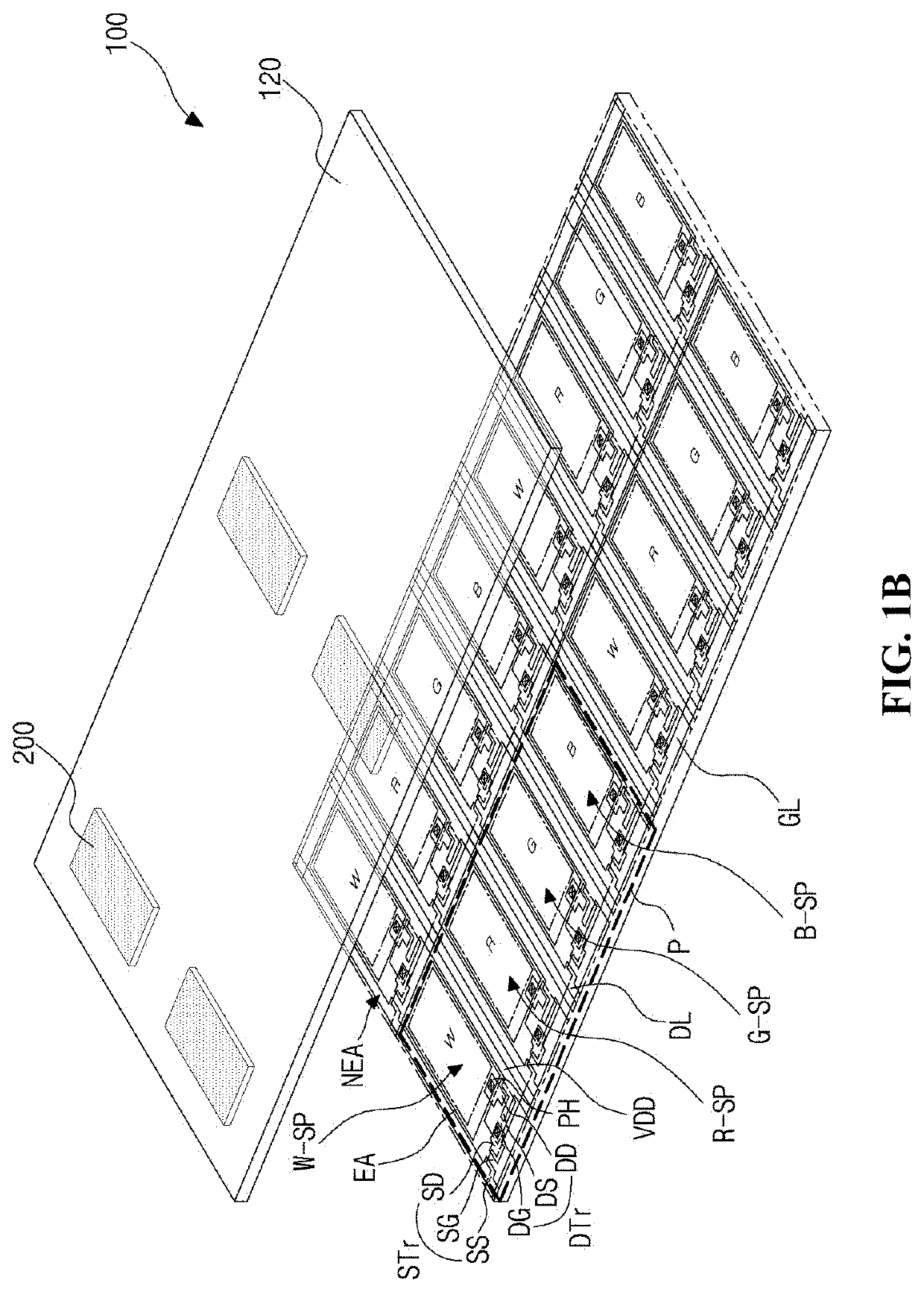
[0029]FIGS. 1A and 1B are plan and perspective views showing a plurality of subpixels in an organic light-emitting diode display device according to a first embodiment of the present disclosure, respectively.

[0030]As shown in FIGS. 1A and 1B, the organic light-emitting diode display device include a plurality of unit pixels P, each of which has red, green and blue subpixels R-SP, G-SP and B-SP. Each subpixel R-SP, G-SP and B-SP includes an emission area EA, and a bank 119 of FIG. 2 is disposed along an edge of the emission area EA to form a non-emission area NEA.

[0031]The red, green and blue subpixels R-SP, G-SP and B-SP may be alternately disposed along a first direction, for example, a horizontal direction in the context of the figures, and a plurality of the red, green or blue subpixels R-SP, G-SP or B-SP, e.g., the same color subpixels may be disposed along a second direction, for example, a vertical direction in the context of the figure.

[0032]Accordingly, the red, green and bl...

second embodiment

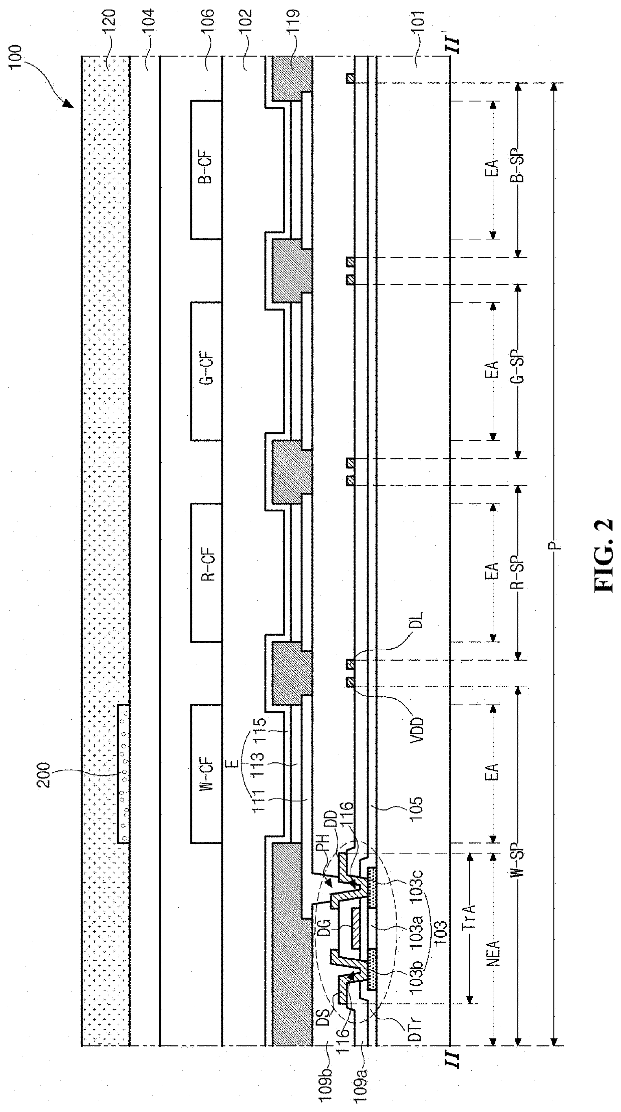
[0151]FIG. 6 is a cross-sectional view of an organic light-emitting diode display device according to a second embodiment of the present disclosure and shows a structure of a unit pixel including four subpixels.

[0152]For convenience of description, the same parts as those of the first embodiment are designated by the same reference signs, and explanation for the same parts will be shortened or omitted.

[0153]In FIG. 6, a driving thin film transistor DTr including a semiconductor layer 103, a gate insulation layer 105, a gate electrode DG, and source and drain electrodes DS and DD is disposed in a switching area TrA of a non-emission area NEA on a substrate 101, and a first electrode 111 connected to the drain electrode DD exposed through a drain contact hole PH, which is formed in the gate insulation layer 105 and a first interlayer insulation layer 109a, is disposed on a second interlayer insulation layer 109b corresponding to an emission area EA.

[0154]At this time, the first electr...

third embodiment

[0174]FIG. 7 is a cross-sectional view of an organic light-emitting diode display device according to a third embodiment of the present disclosure and shows a structure of a unit pixel including four subpixels. The organic light-emitting diode display device according to the third embodiment of the present disclosure is a bottom emission type.

[0175]For convenience of description, the same parts as those of the first and second embodiments are designated by the same reference signs, and explanation for the same parts will be shortened or omitted.

[0176]In FIG. 7, a driving thin film transistor DTr including a semiconductor layer 103, a gate insulation layer 105, a gate electrode DG, and source and drain electrodes DS and DD is disposed in a switching area TrA of a non-emission area NEA on a substrate 101, and white, red, green and blue color filter patterns W-CF, R-CF, G-CF and B-CF are disposed on a first interlayer insulation layer 109a corresponding to emission areas EA of white, r...


PUM

PropertyMeasurementUnit
transmittanceaaaaaaaaaa
hazeaaaaaaaaaa
hazeaaaaaaaaaa

Abstract

The present disclosure relates to an organic light-emitting diode display device that comprises a first substrate on which first, second and third subpixels each including an emission area and a non-emission area are defined; first, second and third light-emitting diodes disposed in the first, second and third subpixels on the first substrate, respectively; a second substrate over the first, second and third light-emitting diodes; and a scattering pattern corresponding to the first subpixel and disposed over the first light-emitting diode or under the first substrate, wherein the first subpixel has an area reflectance higher than the second and third subpixels.

Description

CROSS-REFERENCE TO RELATED APPLICATION[0001]The present application claims priority from and the benefit under 35 U.S.C § 119(a) of Korean Patent Application No. 10-2020-0088135 filed in the Republic of Korea on Jul. 16, 2020, which is hereby incorporated by reference in its entirety.BACKGROUNDTechnical Field[0002]The present disclosure relates to an organic light-emitting diode display device, and more particularly, an organic light-emitting diode display device that can realize low reflection and high brightness and display an image with excellent color tones by preventing the displayed image from being modulated due to reflection of external light.Discussion of the Related Art[0003]Recently, with entering into a full-fledged information age, there is a growing interest in information display dealing with and displaying mass information. In addition, as the demand to use portable information media increases, various lightweight and thin flat panel display devices corresponding to ...

Claims


Application Information

Patent Timeline
Patent Type & Authority Applications(United States)
IPC IPC(8): H01L51/52H01L27/32
CPCH01L51/5268H01L27/3213H01L51/5281H01L27/3244H01L27/322H10K59/351H10K59/38H10K50/854H10K50/865H10K59/35H10K50/86H10K59/12
Inventor CHANG, SU-JINLEE, SUNG-RAEMIN, JU-HUN
Owner LG DISPLAY CO LTD
Why Eureka
Try Eureka