

Solid-state imaging element and imaging device
- Summary
- Abstract
- Description
- Claims
- Application Information
AI Technical Summary
Benefits of technology
Problems solved by technology
Method used
Image

Examples
first embodiment
1. First Embodiment
[0046][Configuration Example of Imaging Device]
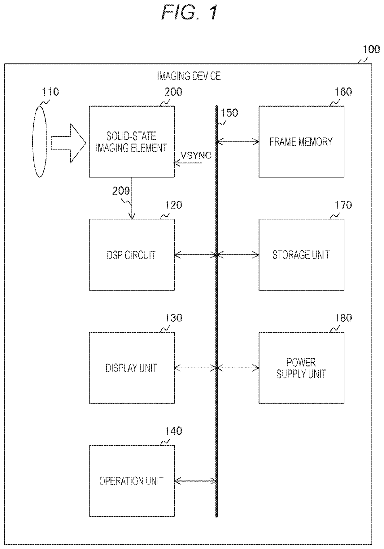
[0047]FIG. 1 is a block diagram illustrating a configuration example of an imaging device 100 in a first embodiment of the present technology. The imaging device 100 is a device for imaging image data, and is provided with an optical unit 110, a solid-state imaging element 200, and a digital signal processing (DSP) circuit 120. The imaging device 100 is further provided with a display unit 130, an operation unit 140, a bus 150, a frame memory 160, a storage unit 170, and a power supply unit 180. As the imaging device 100, for example, in addition to a digital camera such as a digital still camera, a smartphone and a personal computer having an imaging function, an in-vehicle camera and the like are assumed.
[0048]The optical unit 110 condenses light from a subject and guides the same to the solid-state imaging element 200. The solid-state imaging element 200 generates the image data by photoelectric conversion in synch...
second embodiment
2. Second Embodiment
[0176]In the second embodiment described above, six transistors are arranged in every normal pixel 310, but as the number of pixels increases, the circuit scale of the pixel array unit 300 increases. A solid-state imaging element 200 in a second embodiment is different from that in the first embodiment in that a circuit scale of a normal pixel 310 is reduced.
[0177]FIG. 22 is a circuit diagram illustrating a configuration example of the normal pixel 310 in the second embodiment of the present technology. The normal pixel 310 is different from that in the first embodiment in that a discharge transistor 311, an analog memory 314, and a transfer transistor 315 are not arranged.
[0178]Furthermore, a transfer transistor 313 in the second embodiment transfers electric charge from a photodiode 312 to a floating diffusion layer 316 in accordance with a transfer signal TX.
[0179]FIG. 23 is a timing chart illustrating an example of an imaging operation of the solid-state imag...
PUM
 Abstract
Description
Claims
Application Information