Display panel, preparing method thereof, and display device

a display panel and preparing method technology, applied in the field of displays, can solve the problems of large difference, high consumption of time and material costs, and yield loss to a certain degree, and achieve the effects of improving the conduction characteristics of the thin film transistor, enhancing the contact quality of the edge, and improving the conduction performance of the sour

Active Publication Date: 2022-02-10
SHENZHEN CHINA STAR OPTOELECTRONICS SEMICON DISPLAY TECH CO LTD
View PDF0 Cites 1 Cited by
  • Summary
  • Abstract
  • Description
  • Claims
  • Application Information

AI Technical Summary

Benefits of technology

[0025]A display panel provided by an embodiment of the present disclosure has a source and a drain both of which have a width smaller than that of the active layer. By increasing a conductorized area of the active layer, paths of the active layer contacting edges of the source and the drain increase. By using a lateral diffusion phenomenon when the active layer is conductorized, the edge contact quality of the source, the drain, and the active layer is enhanced, thereby greatly improving conduction characteristics of the thin film transistor, improving and optimizing conduction performances of the source, the drain and the active layer in the thin film transistor in which the source, the gate, and the drain are prepared in a same layer. Mass production can be realized.

Problems solved by technology

At present, a thin-film transistor with a top gate structure has a complicated structure and a large number of layers, resulting in high consumption of time costs and material costs, as well as yield loss to a certain degree.
Therefore, it is necessary to develop a thin film transistor with a top gate with few preparing processes and desired device functions.
Compared with the number of old processes for preparing the thin-film transistor with the top-gate structure, the new processes save metal film formation, photolithography, etching and interlayer insulating layer formation one time, and greatly saves costs, but there is a large difference, compared with the old processes for preparing the thin-film transistor with the top gate structure, especially an active layer.
Because materials of the source, gate and drain are low-impedance metals, dry etching cannot be used.
During a wet etching process, a metal etching solution continuously contacts the active layer, resulting in serious damage to a thickness of the active layer, contact resistance, etc.
The active layer is subjected to the dry etching processes of the gate insulating layer twice, thereby also damaging the active layer, making the source, the drain and the active layer fail to conduct, and failing to achieve the function of the thin film transistor.

Method used


Image

  • Display panel, preparing method thereof, and display device
  • Display panel, preparing method thereof, and display device
  • Display panel, preparing method thereof, and display device

Examples


first embodiment

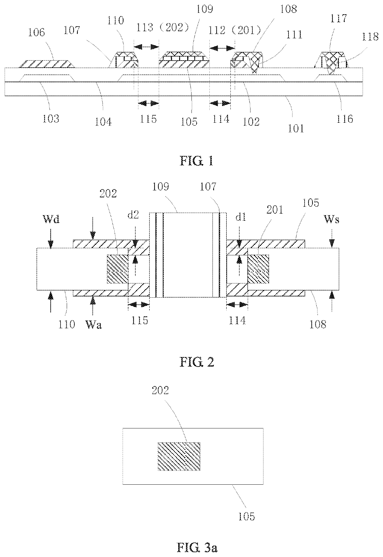
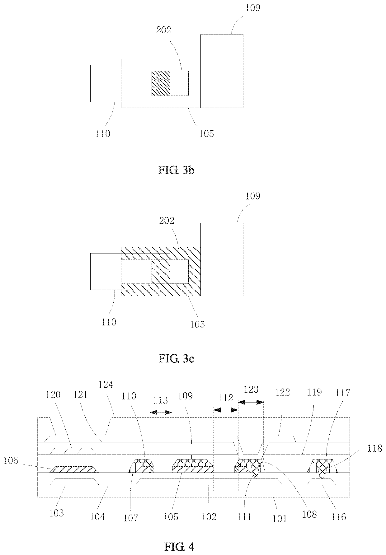
[0032]Refer to FIG. 1, which is a schematic diagram of a basic structure of a display panel provided in the present disclosure. From the figure, the components of the present disclosure and the relative positional relationship between the components can be seen intuitively. The display panel includes a substrate layer 101; a light shielding metal layer 102 and a first electrode plate 103 of a storage capacitor on the substrate layer 101; a buffer layer 104 covering the light shielding metal layer 102 and the first electrode plate 103 on the substrate layer 101; an active layer 105 and a second electrode plate 106 of the storage capacitor on the buffer layer 104; a gate insulating layer 107 on the buffer layer 104 and the active layer 105; and a source 108, a gate 109 and a drain 110 on the gate insulating layer 107; wherein the source 108 is connected to the light shielding metal layer 102 through a first via hole 111. A second via hole 112 and a third via hole 113 are defined by th...

second embodiment

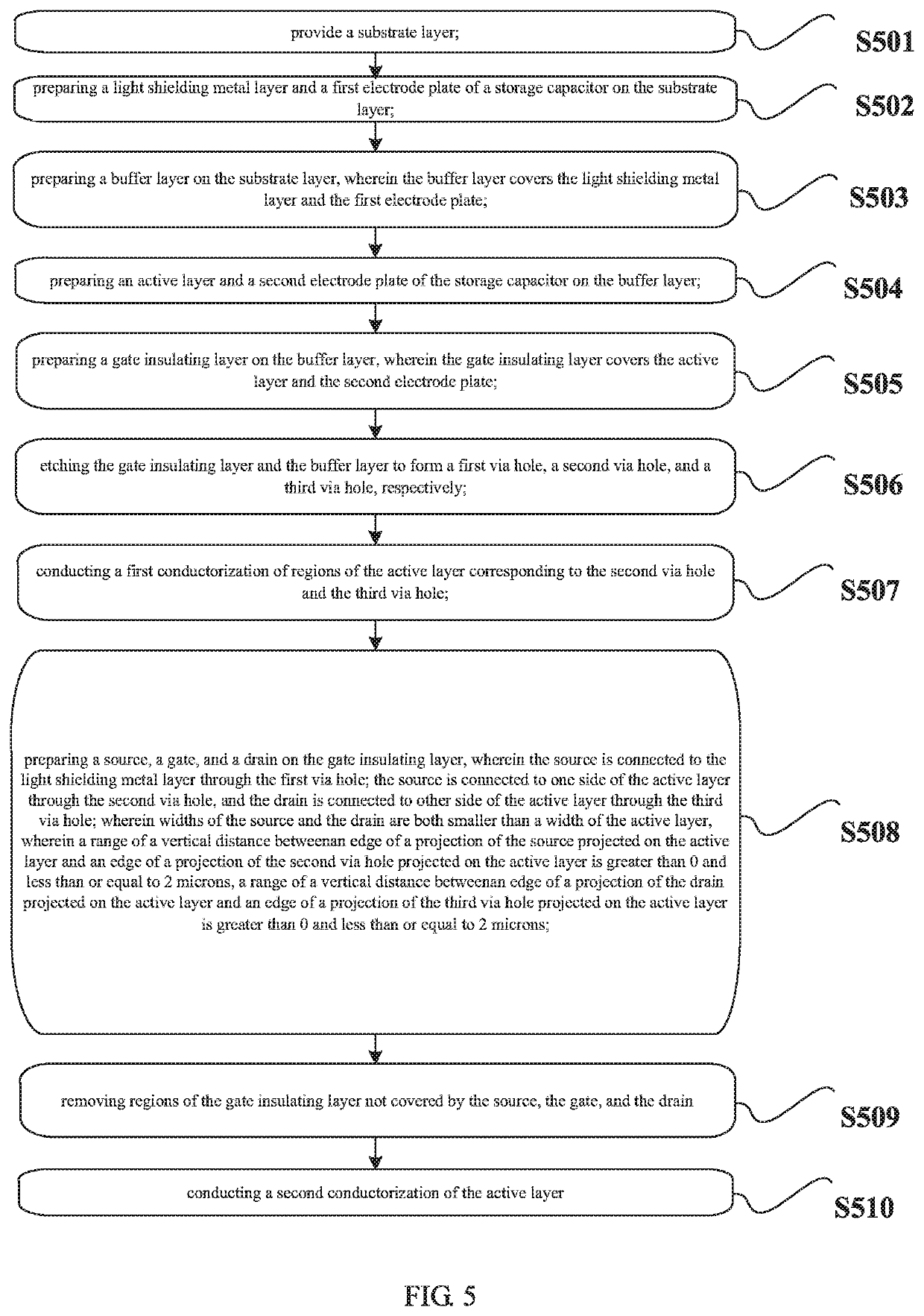
[0043]Refer to FIG. 4, which is a schematic diagram of a basic structure of a display panel provided in the present disclosure. From the figure, the components of the present disclosure and the relative positional relationship between the components can be seen intuitively. The display panel includes a substrate layer 101; a light shielding metal layer 102 and a first electrode plate 103 of a storage capacitor on the substrate layer 101; a buffer layer 104 covering the light shielding metal layer 102 and the first electrode plate 103 on the substrate layer 101; an active layer 105 and a second electrode plate 106 of the storage capacitor on the buffer layer 104; a gate insulating layer 107 on the buffer layer 104 and the active layer 105; and a source 108, a gate 109, and a drain 110 on the gate insulating layer 107; wherein the source 108 is connected to the light shielding metal layer 102 through a first via hole 111. A second via hole 112 and a third via hole 113 are defined by t...


PUM

PropertyMeasurementUnit
vertical distanceaaaaaaaaaa
vertical distance d1aaaaaaaaaa
vertical distance d2aaaaaaaaaa

Abstract

A display panel, a method for preparing a display panel, and a display device are disclosed. The display panel includes a substrate layer; a light shielding metal layer and a first electrode plate of a storage capacitor on the substrate layer; a buffer layer covering the light shielding metal layer and the first electrode plate on the substrate layer; an active layer and a second electrode plate of the storage capacitor on the buffer layer; a gate insulating layer on the buffer layer and the active layer, and a source, a gate and a drain on the gate insulating layer.

Description

FIELD OF INVENTION[0001]The present disclosure relates to the technical field of displays, and in particular to a display panel, a preparing method thereof, and a display device.BACKGROUND OF DISCLOSURE[0002]At present, a thin-film transistor with a top gate structure has a complicated structure and a large number of layers, resulting in high consumption of time costs and material costs, as well as yield loss to a certain degree. Therefore, it is necessary to develop a thin film transistor with a top gate with few preparing processes and desired device functions.[0003]In a conventional technique, new processes for preparing a source, a gate and a drain in a same layer are employed to prepare the display panel. Compared with the number of old processes for preparing the thin-film transistor with the top-gate structure, the new processes save metal film formation, photolithography, etching and interlayer insulating layer formation one time, and greatly saves costs, but there is a larg...

Claims


Application Information

Patent Timeline
Patent Type & Authority Applications(United States)
IPC IPC(8): H01L27/32H01L51/52H01L51/56
CPCH01L27/3272H01L27/3258H01L27/3265H01L2251/308H01L51/5253H01L51/56H01L27/3246H01L27/1222H01L27/1225H01L27/1255H01L27/1259H01L27/127H01L21/77H10K59/1213H10K59/1201H01L29/41733H01L29/78633H10K59/1216H10K59/126H01L29/78618H10K50/844H10K59/122H10K59/124H10K71/00H10K2102/103
Inventor TANG, JIA
Owner SHENZHEN CHINA STAR OPTOELECTRONICS SEMICON DISPLAY TECH CO LTD
Why Eureka
Try Eureka