Display panel having increased conductorized area of an active layer, preparing method thereof, and display device employing the display panel
a display panel and active layer technology, applied in the field of displays, can solve the problems of large difference, high consumption of time and material costs, and yield loss to a certain degree, and achieve the effects of improving the conduction characteristics of the thin film transistor, enhancing the contact quality of the edge, and optimizing the conduction performance of the sour
- Summary
- Abstract
- Description
- Claims
- Application Information
AI Technical Summary
Benefits of technology
Problems solved by technology
Method used
Image
Examples
first embodiment
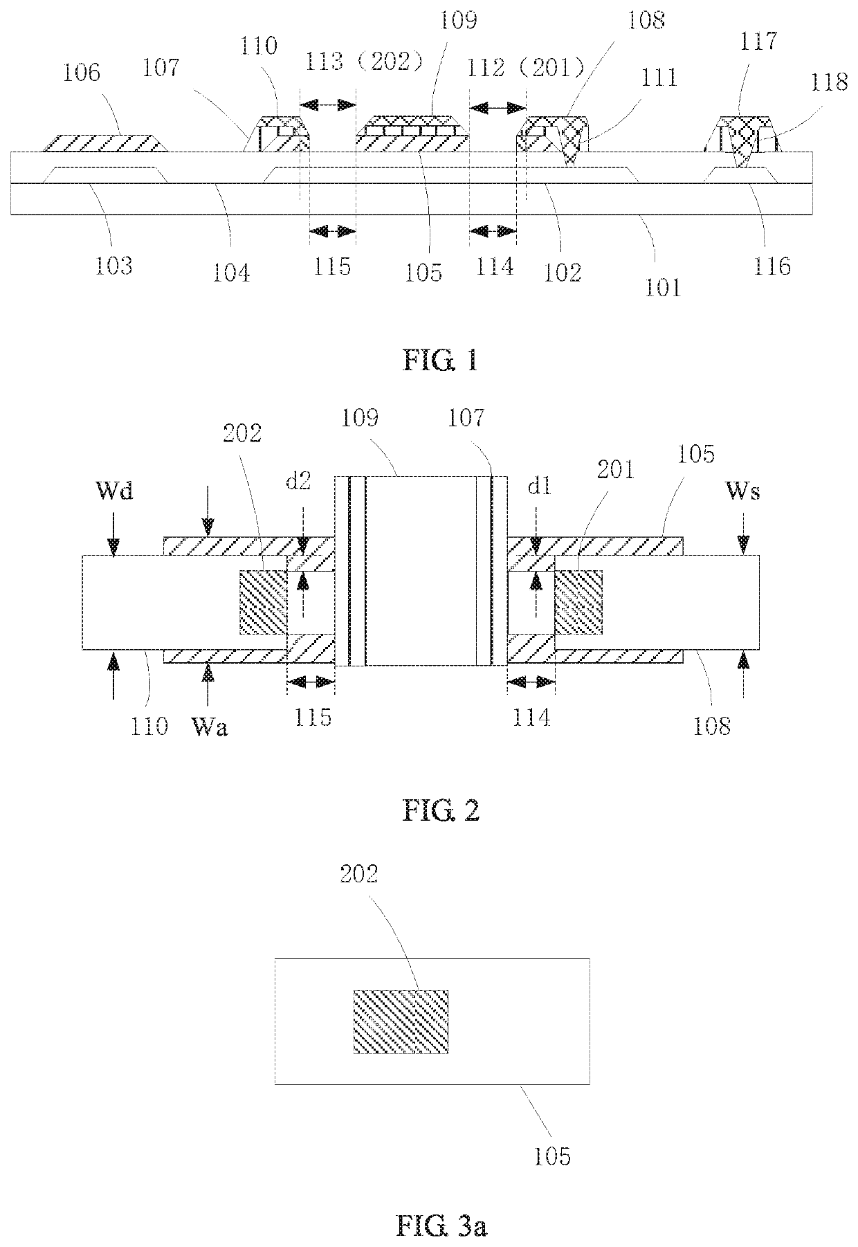
[0033]Refer to FIG. 1, which is a schematic diagram of a basic structure of a display panel provided in the present disclosure. From the figure, the components of the present disclosure and the relative positional relationship between the components can be seen intuitively. The display panel includes a substrate layer 101; a light shielding metal layer 102 and a first electrode plate 103 of a storage capacitor on the substrate layer 101; a buffer layer 104 covering the light shielding metal layer 102 and the first electrode plate 103 on the substrate layer 101; an active layer 105 and a second electrode plate 106 of the storage capacitor on the buffer layer 104; a gate insulating layer 107 on the buffer layer 104 and the active layer 105; and a source 108, a gate 109 and a drain 110 on the gate insulating layer 107; wherein the source 108 is connected to the light shielding metal layer 102 through a first via hole 111. A second via hole 112 and a third via hole 113 are defined by th...
second embodiment
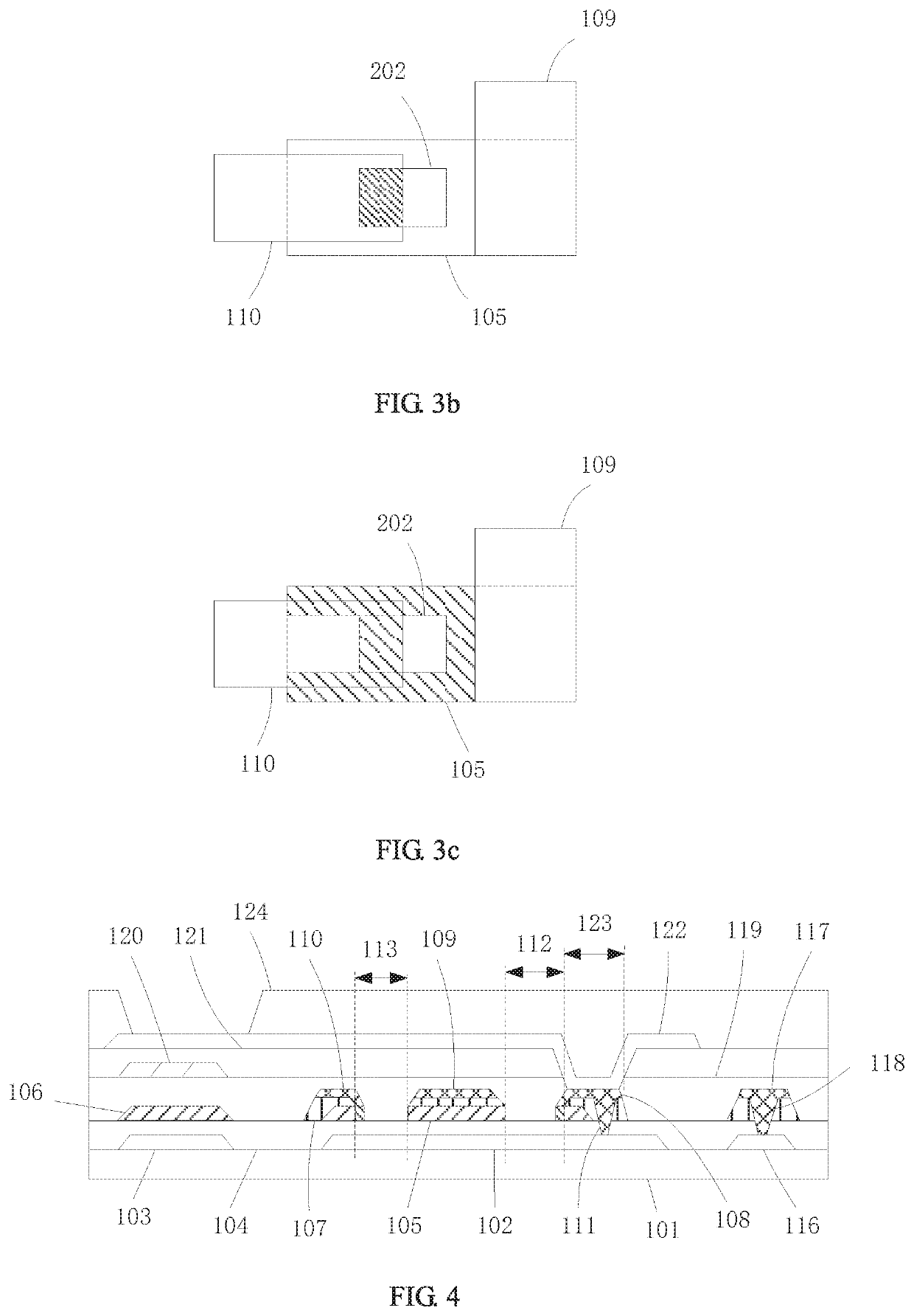
[0044]Refer to FIG. 4, which is a schematic diagram of a basic structure of a display panel provided in the present disclosure. From the figure, the components of the present disclosure and the relative positional relationship between the components can be seen intuitively. The display panel includes a substrate layer 101; a light shielding metal layer 102 and a first electrode plate 103 of a storage capacitor on the substrate layer 101; a buffer layer 104 covering the light shielding metal layer 102 and the first electrode plate 103 on the substrate layer 101; an active layer 105 and a second electrode plate 106 of the storage capacitor on the buffer layer 104; a gate insulating layer 107 on the buffer layer 104 and the active layer 105; and a source 108, a gate 109, and a drain 110 on the gate insulating layer 107; wherein the source 108 is connected to the light shielding metal layer 102 through a first via hole 111. A second via hole 112 and a third via hole 113 are defined by t...
PUM
| Property | Measurement | Unit |
|---|---|---|
| vertical distance | aaaaa | aaaaa |
| vertical distance d1 | aaaaa | aaaaa |
| vertical distance d2 | aaaaa | aaaaa |
Abstract
Description
Claims
Application Information


