Piezoelectric device with piezoelectric elongate nano-objects

a piezoelectric and nano-object technology, applied in the field of piezoelectric devices, can solve problems such as the absence of matrix, and achieve the effect of satisfactory freedom of deformation good strength of piezoelectric elongate nano-objects

Pending Publication Date: 2022-03-10
COMMISSARIAT A LENERGIE ATOMIQUE ET AUX ENERGIES ALTERNATIVES +3
View PDF0 Cites 0 Cited by
  • Summary
  • Abstract
  • Description
  • Claims
  • Application Information

AI Technical Summary

Benefits of technology

[0017]The use of the first and second layers having different thicknesses and respectively formed by a first material and by a second material with different Young's moduli allows ensuring different holdings of the piezoelectric elongate nano-objects between the first and second electrodes. Th

Problems solved by technology

However, the tradeoff is generally achieved by favoring the deformation capability of the piezoelectric nanowires secured to the substrate at the expense of a good strength of the array of piezoelectric nanowires.
Such a polymer matrix does not

Method used


Image

  • Piezoelectric device with piezoelectric elongate nano-objects
  • Piezoelectric device with piezoelectric elongate nano-objects
  • Piezoelectric device with piezoelectric elongate nano-objects

Examples


first embodiment

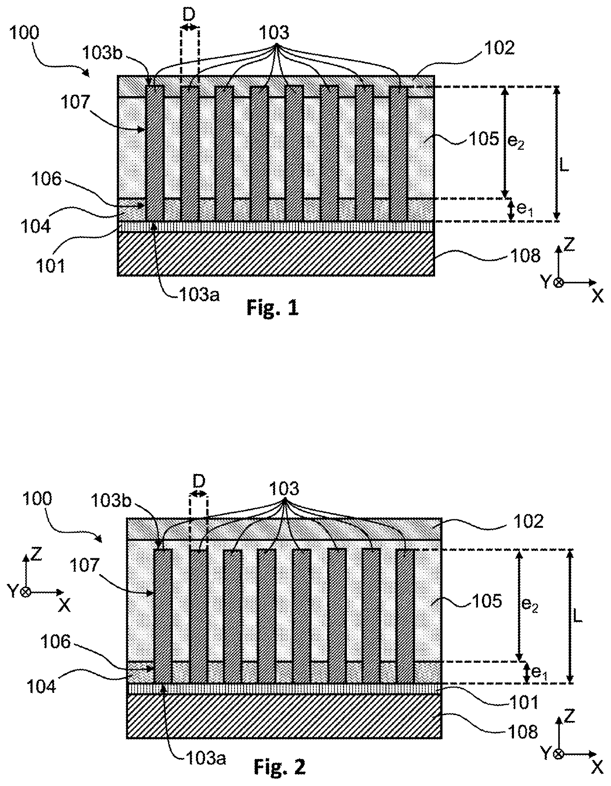
[0117]To obtain the piezoelectric device 100 according to this first embodiment, the step of forming the second layer 105 is such that it leaves the second longitudinal ends 103b of the piezoelectric elongate nano-objects 103 accessible in order to enable the formation of the second electrode 102 in contact with these second longitudinal ends 103b. In other words, on completion of the formation of the second layer 105, portions of each of the piezoelectric elongate nano-objects 103 protrude from the second layer 105 as shown for example in FIG. 6. Afterwards, the second electrode 102 is formed on the second layer 105 and is in contact with the portions of the piezoelectric elongate nano-objects 103 protruding from the second layer 105 as shown in FIG. 1.

[0118]According to the first embodiment, it is possible to distinguish two cases:[0119]if the interface between the first electrode 101 and the piezoelectric elongate nano-objects 103 is of the ohmic type then the interface between t...

second embodiment

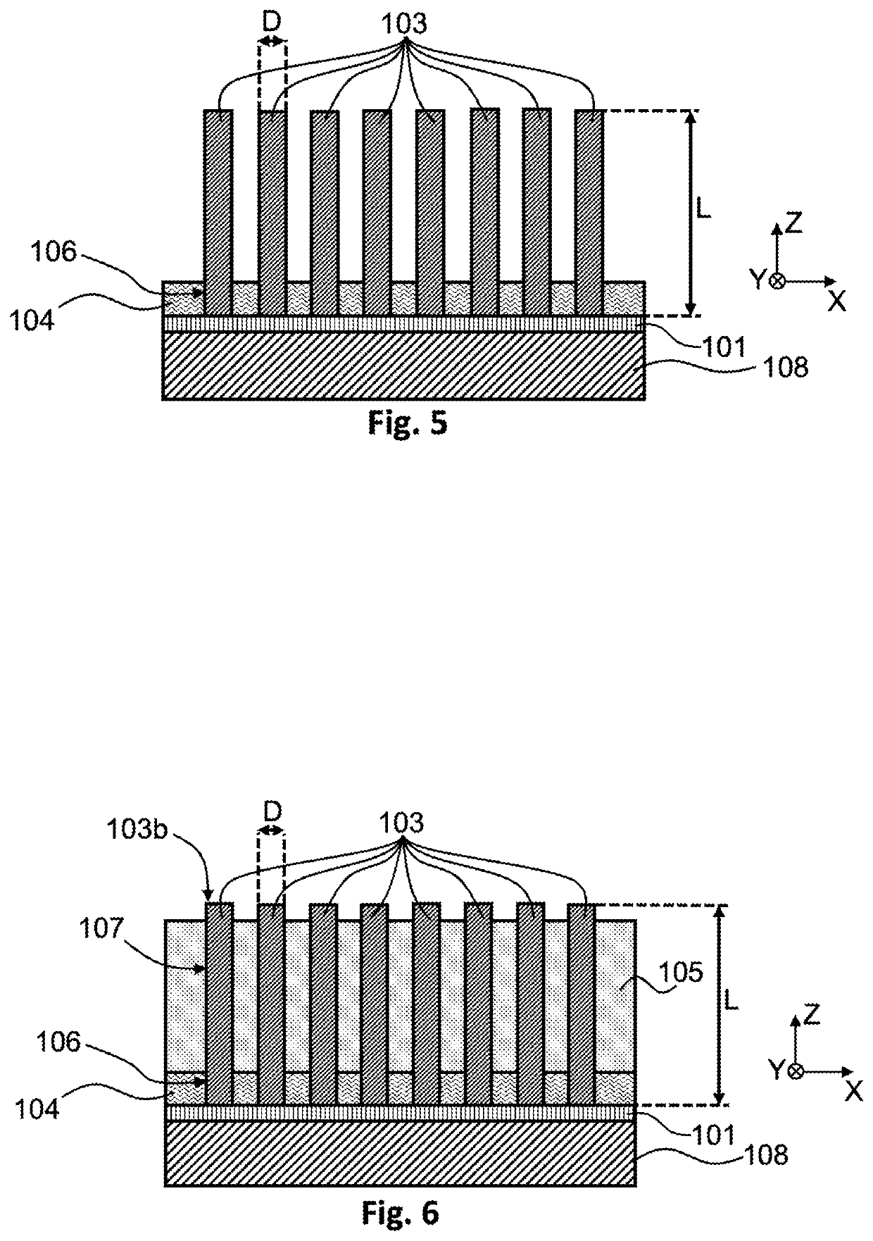
[0127]Thus, according to this second embodiment, the second longitudinal end 103b of each of the piezoelectric elongate nano-objects 103 is embedded by the second material of the second layer 105.

[0128]In the second embodiment, there is no particular criterion on the nature of the interface between the second layer 105 and the second layer 102. Henceforth, the second electrode 102 may be formed by any metal that could in particular be deposited by PVD.

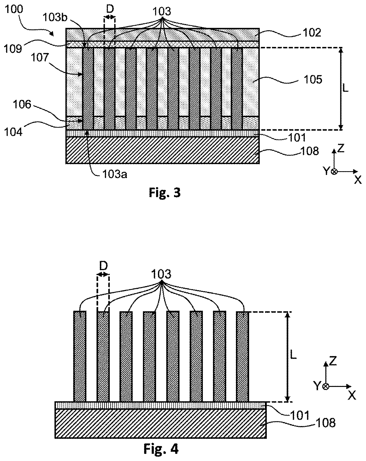
[0129]According to the third embodiment, as illustrated for example in FIG. 3, the first longitudinal ends 103a of the piezoelectric elongate nano-objects 103 are in contact with the first electrode 101, and the second longitudinal ends 103b of the piezoelectric elongate nano-objects 103 are in contact with a third layer 109 of an electrically-insulating material also called dielectric layer 109. The third layer 109 connects the second longitudinal ends 103b to the second layer 102. This particular arrangement including the first, seco...

third embodiment

[0130]For this third embodiment, there is no particular criterion on the nature of the interface between the third layer 109 and the second layer 102. Henceforth, the second electrode 101 may be formed by any metal that could in particular be deposited by PVD.

[0131]The electrically-insulating material of the third layer 109 may have a high relative permittivity εr, that is to say higher than or equal to 3.9. In particular, the electrically-insulating material of the third layer 109 may be selected amongst an aluminum oxide like alumina such as Al2O3 or its non-stoichiometric derivatives, a silicon nitride such as for example Si3N4 or its non-stoichiometric derivatives, or a hafnium oxide such as HfO2 or its non-stoichiometric derivatives. This allowing in particular improving the collection of charges by the second electrode 102 during the use of the piezoelectric device 100.

[0132]The thickness of the third layer 109 may be comprised between 10 nm and 100 nm, this thickness allowing...


PUM


Abstract

The piezoelectric device includes a first electrode, a second electrode, piezoelectric elongate nano-objects in contact with the first electrode, and extending between the first electrode and the second electrode, a first layer of an electrically-insulating first material, the first layer surrounding a first longitudinal portion of each of the piezoelectric elongate nano-objects, a second layer of an electrically-insulating second material, the second layer surrounding a second longitudinal portion of each of the piezoelectric elongate nano-objects. The first layer is arranged between the first electrode and the second layer. The thickness of the first layer is strictly smaller than the thickness of the second layer. The first material has a Young's modulus strictly higher than the Young's modulus of the second material.

Description

TECHNICAL FIELD OF THE INVENTION[0001]The technical field of the invention concerns piezoelectricity and in particular a piezoelectric device, such as for example a piezoelectric nanogenerator, including piezoelectric elongate nano-objects such as for example nanowires.STATE OF THE ART[0002]A piezoelectric nanogenerator, also known under the abbreviation PENG, can generate an electric voltage from mechanical vibrations applied to the piezoelectric nanogenerator. The piezoelectric nanogenerator is a transducer. The piezoelectric nanogenerators are of great interest in the development of low-power portable electronic systems as they could be miniaturized and because they allow making these portable electronic systems energy self-sufficient.[0003]The piezoelectric nanogenerator may be formed according to vertical integrated nanogenerator type, also known under the abbreviation «VING», architecture. To form the nanogenerator according to this VING-type architecture, an array of piezoele...

Claims


Application Information

Patent Timeline
IPC IPC(8): H01L41/09H01L41/187H01L41/22H01L41/113
CPCH01L41/0986H01L41/113H01L41/22H01L41/187H10N30/30H10N30/01H10N30/206H10N30/853
Inventor LAUSECKER, CLÉMENTBAILLIN, XAVIERCONSONNI, VINCENTSALEM, BASSEM
Owner COMMISSARIAT A LENERGIE ATOMIQUE ET AUX ENERGIES ALTERNATIVES
Why Eureka
Try Eureka