Structure of memory module and modification method of memory module

a technology of memory modules and structure, applied in the direction of printed circuits, printed circuit aspects, programable/customizable/modifiable circuits, etc., can solve the problems of wasting resources, increasing costs, and a lot of operation time, and achieve the effect of improving the structure of memory modules

Active Publication Date: 2022-03-17
LIEN SHIH HSIUNG
View PDF5 Cites 0 Cited by
  • Summary
  • Abstract
  • Description
  • Claims
  • Application Information

AI Technical Summary

Benefits of technology

[0007]The primary objective of the present invention is to provide an improved memory module structure and a memory module modification method, which help alleviate and overcome the problems discussed above, in which a conduction element or a conductor line is used to electrically connect solder pads for electrically connecting the memory units and the connection interface, so that the operation and time that a manufacturer or a distributor must take to modify and convert a register-included dual inline memory module into the improved structure can be saved, and also, there is no need to provide an additional, new printed circuit board and to dispose of an existing printed circuit board of the register-included dual inline memory module to thereby eliminating waste of resources.

Problems solved by technology

However, with the development of the market, there is sometimes an issue of surplus supply of RDIMMs, and as such, the manufacturers or the suppliers were intending to modify and convert RDIMMs, FBDIMMs, or LRDIMMS into UDIMMS or SODIMMs.
However, an operation of modification, if implemented as noted above, would make it necessary for a manufacturer or a supplier to spend a lot of operation time for the removing and re-mounting job.
In addition, the printed circuit board is not shareable between the two and this inevitably leads to an increase in cost and a waste of resources.

Method used


Image

  • Structure of memory module and modification method of memory module
  • Structure of memory module and modification method of memory module
  • Structure of memory module and modification method of memory module

Examples


Embodiment Construction

[0031]Embodiments of the present invention will be described below with reference to FIGS. 1-8. The description is not intended to impose undue constraints to the ways of embodying the present invention, and is rather provided as one way of embodying the present invention.

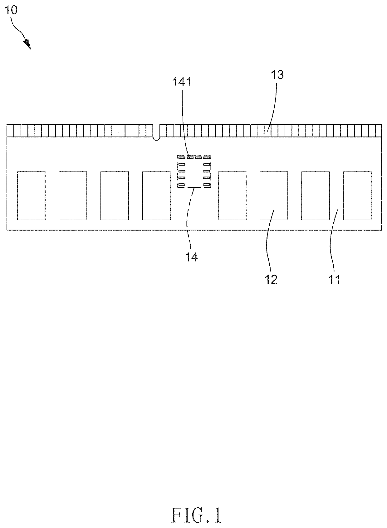
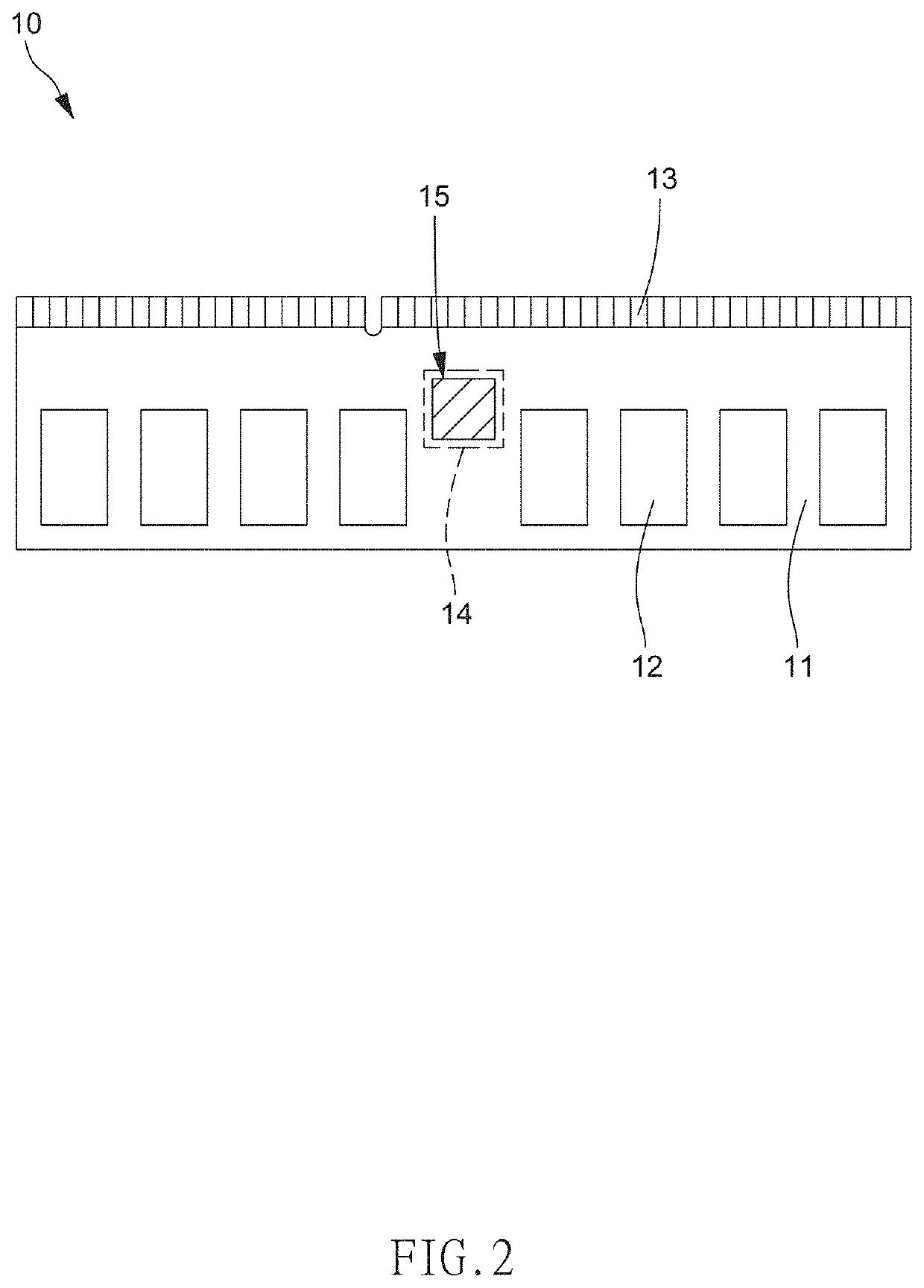
[0032]Firstly, referring simultaneously to FIGS. 1 and 2, the present invention provides an improved memory module structure 10, which comprises: a printed circuit board 11; a plurality of memory units 12, the memory units 12 being disposed on the printed circuit board 11; and a connection interface 13, which is disposed on the printed circuit board 11 for connection with a host system of an electronic device (not shown). The printed circuit board 11 is provided with a solder pad zone 14 that is in electrical connection with the memory units 12 and the connection interface 13. The solder pad zone 14 includes a plurality of solder pads 141. A conduction element 15 is combinable with the solder pad zone 14, so as to ...


PUM


Abstract

An improved memory module structure includes a printed circuit board, memory units disposed on the printed circuit board, and a connection interface disposed on the printed circuit board for connection with an electronic device. The printed circuit board includes a solder pad zone having solder pads electrically connected with the memory units and the connection interface. A conduction element is combined with the solder pad zone or at least one conductor line electrically connected, in the form of bridge connection, the solder pads, in order to have the solder pads electrically connected. A memory module modification method is also provided, including removing a register from an existing dual inline memory module to expose a solder pad zone, and disposing of a conduction element or arranging a conductor line to have the memory units and the connection interface of electrically connected to thereby form an improved memory module structure.

Description

CROSS-REFERENCE TO RELATED APPLICATION[0001]The application claims the priority of Taiwan Patent Application Nos. 109131898 and 110205718, which were filed on Sep. 16, 2020 and May 19, 2021, respectively.FIELD OF THE INVENTION[0002]The present invention relates to a technical field concerning memory modules and modification methods thereof, and more particular to an improved memory module structure that enhances modification thereof and a memory module modification method that modifies a dual-inline memory module with a register into an improved memory module structure.BACKGROUND OF THE INVENTION[0003]The up-to-date development of integrated circuits makes it necessary to include a memory module in an electronic device in order to store or temporarily hold and cache digital data. Various memory modules that are currently available are generally classified as unbuffered dual inline memory module (UDIMM), registered dual inline memory module (RDIMM), small outline dual inline memory m...

Claims


Application Information

Patent Timeline
Patent Type & Authority Applications(United States)
IPC IPC(8): H05K1/11H05K1/02
CPCH05K1/111H05K2201/10159H05K1/0203H05K1/0286H05K2203/173H05K2203/176H05K2201/10204
Inventor LIEN, SHIH-HSIUNG
Owner LIEN SHIH HSIUNG
Why Eureka
Try Eureka