Method for producing ceramic electronic component

Pending Publication Date: 2022-03-24
MURATA MFG CO LTD
View PDF0 Cites 3 Cited by
  • Summary
  • Abstract
  • Description
  • Claims
  • Application Information

AI Technical Summary

Benefits of technology

The present invention provides methods for producing ceramic electronic components with outer electrodes that can withstand external mechanical or thermal stresses without losing their performance. This is achieved by forming metal and glass portions in the baked electrode layer, which help to reduce cracks that may occur when the component is subjected to external stresses. Additionally, the method minimizes chipping and cracking of the ceramic body during processing.

Problems solved by technology

However, as a result of the barrel processing or blast processing, cracks starting from the boundaries between the metal portions and the glass portions and extending toward the inner side of the glass portions are formed in the glass portions in the baked electrode layer.

Method used


Image

  • Method for producing ceramic electronic component
  • Method for producing ceramic electronic component

Examples


Embodiment Construction

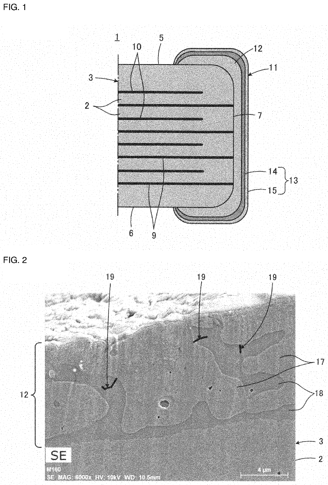
[0018]To explain a ceramic electronic component produced using the production methods according to preferred embodiments of the present invention, a multilayer ceramic capacitor is used as an example of the ceramic electronic component.

[0019]Referring to FIG. 1, the multilayer ceramic capacitor 1 includes a ceramic body 3 including a plurality of laminated ceramic layers 2 made of a dielectric ceramic. The ceramic body includes a first principal surface 5 and a second principal surface 6 that are opposed to each other and a first end surface 7 connecting these principal surfaces, an unillustrated second end surface opposed to the first end surface 7, and unillustrated first and second side surfaces extending parallel or substantially parallel to the drawing sheet in FIG. 1 and opposed to each other.

[0020]The ceramic body 3 further includes a plurality of first inner electrodes 9 and a plurality of second inner electrodes 10 that are disposed along a plurality of boundaries between t...


PUM

PropertyMeasurementUnit
Percent by volumeaaaaaaaaaa
Particle sizeaaaaaaaaaa

Abstract

A method for producing a ceramic electronic component includes providing an outer electrode, which includes forming a baked electrode layer by applying an electrically conductive paste including an electrically conductive metal and glass such that the electrically conductive paste covers an exposed portion of an inner electrode on a ceramic body and baking the applied electrically conductive paste, and forming a plating film on the surface of the baked electrode layer by electroplating. The baked electrode layer includes metal portions and glass portions distributed in contact with the metal portions. After the formation of the baked electrode layer, the surface of the baked electrode layer is subjected to barrel or blast processing using a powder having a Mohs hardness equal to or lower than that of the ceramic body.

Description

CROSS REFERENCE TO RELATED APPLICATIONS[0001]This application claims the benefit of priority to Japanese Patent Application No. 2020-157975 filed on Sep. 19, 2020. The entire contents of this application are hereby incorporated herein by reference.BACKGROUND OF THE INVENTION1. Field of the Invention[0002]The present invention relates to a method for producing a ceramic electronic component and, more particularly, to a method for forming an outer electrode on a surface of a ceramic body included in a ceramic electronic component.2. Description of the Related Art[0003]A chip ceramic electronic component, such as a multilayer ceramic capacitor, includes a ceramic body including inner electrodes partially exposed at the surface of the ceramic body, and outer electrodes disposed on a portion of the surface of the ceramic body and electrically connected to the inner electrodes. Each outer electrode includes a baked electrode layer containing an electrically conductive metal such as copper...

Claims


Application Information

Patent Timeline
IPC IPC(8): H01G4/12H01G4/30
CPCH01G4/12H01G4/30H01G4/306H01G4/005H01G4/008H01G4/2325H01G4/232
Inventor KISUMI, TETSUYAYOKOTA, YUSUKE
Owner MURATA MFG CO LTD
Why Eureka
Try Eureka