Plastic optical element with gas barrier film, its manufacturing method and optical pickup device employing the element

Inactive Publication Date: 2009-04-30
KONICA MINOLTA INC
View PDF11 Cites 5 Cited by
  • Summary
  • Abstract
  • Description
  • Claims
  • Application Information

AI Technical Summary

Benefits of technology

[0025]The present invention provides a plastic optical element with a gas barrier film comprising a ceramic layer with excellent adhesion to a substrate, less cracks, high density and high durability, a manufacturing method of a plastic optical element with a gas barrier film providing high durability, and an optical pickup device with excellent pickup property employing the plastic optical element.

Problems solved by technology

When a plastic material is applied as material for an optical element, volume shrinkage or expansion occurs depending on circumstances under which the optical element is used, due to temperature elevation or humidity absorption, and cracks occur in an anti-reflection film provided on the plastic material.
This method is effective for a specific material, however, it is specific and insufficient in adhesion for a material containing cyclicolefin usually used in an optical pickup device, and does not prevent cracks from occurring.
When even an optical element obtained from a combination of techniques disclosed in Patent documents 1, 2 and 3 is exposed to such a light with such a short wavelength, deterioration such as generation of white turbidity or variation of refractive index occurs.
This shortens lifetime of the optical element, and requires exchange of the optical element.

Method used


Image

  • Plastic optical element with gas barrier film, its manufacturing method and optical pickup device employing the element
  • Plastic optical element with gas barrier film, its manufacturing method and optical pickup device employing the element
  • Plastic optical element with gas barrier film, its manufacturing method and optical pickup device employing the element

Examples


example 1

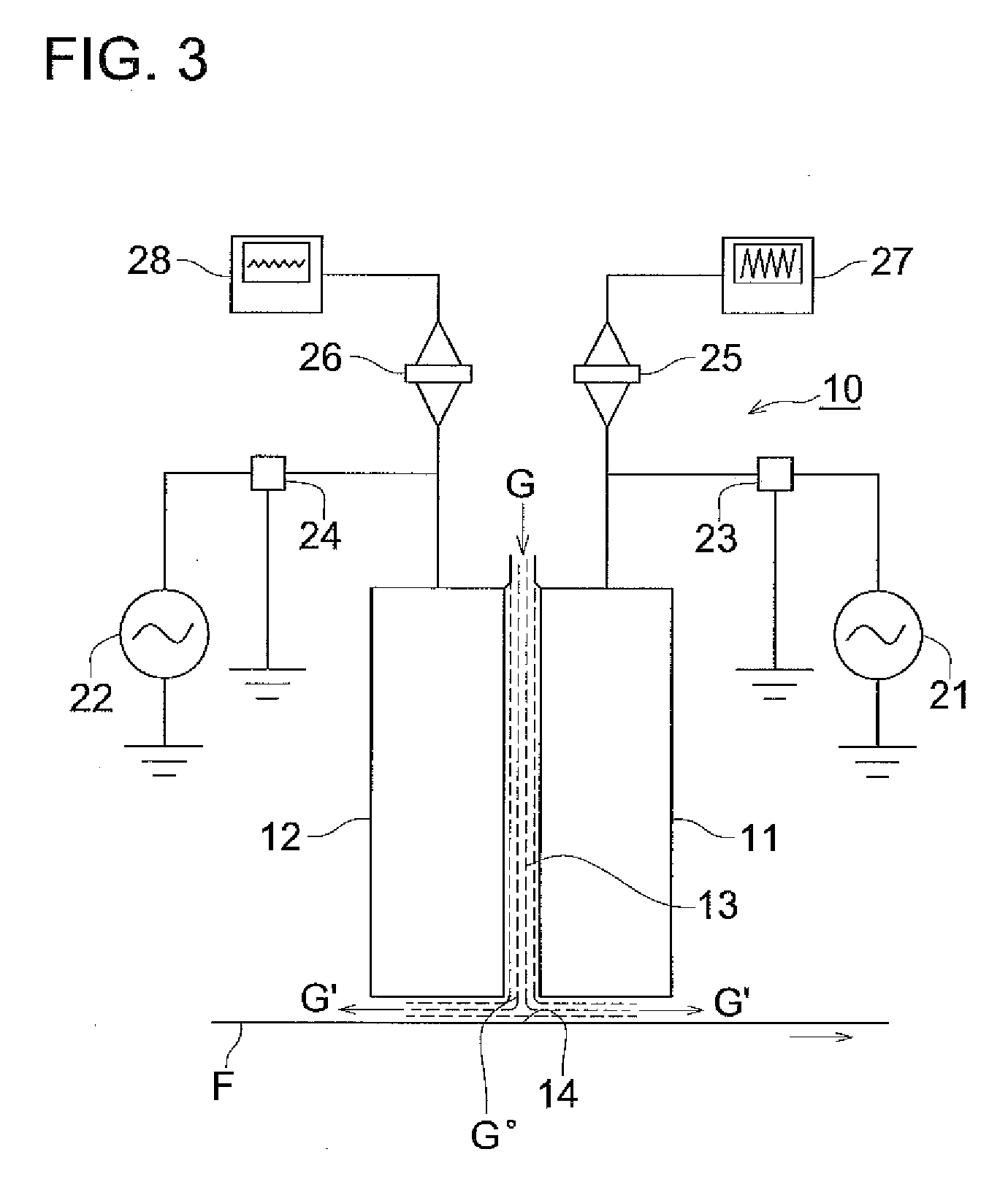
[0171]Plasma discharge processing was performed using the stage electrode type discharge processing apparatus shown in FIG. 4, and a ceramic layer was formed on a substrate described below. In the discharge processing apparatus, a plurality of rod-like electrodes were arranged facing the stage electrode in parallel with the transporting direction of the substrate in such a way that materials (discharge gas, reaction gas 1, 2 described later) and electric power can be supplied to each electrode.

[0172]The dielectric for coating each electrode, together with the opposing electrode, was coated on the ceramic spray electrode to a thickness of 1 mm on one side. After coating, the gap between the electrodes was set to 1 mm. Further, the base metal coating the dielectric was designed as a stainless steel jacket having a cooling function by coolant. Electrode temperature was controlled by coolant during the process of discharging. The light source used in this case was a high frequency power...

example 2

[0187]A layer having the following layer structure was formed on the substrate according to the same procedure in the same manner as in Example 1, using a Plasma CVD apparatus, Model PD-270STP produced by Samco Inc.

[0188]Each layer in Samples Nos. 6 through 10 was formed as follows:

[0189]Oxygen pressure: Gas pressure was changed between 13.3 and 133 Pa as shown in Table 2.

Reaction gas: Tetraethoxy silane (TEOS) at 5 sccm (standard cubic centimeter per minute)

Power: 100W at 13.56 MHz

[0190]Retained substrate temperature: 120° C.

[0191]Samples Nos. 6 through 10 had a ceramic layer with a composition of SiO2, and had a density of 2.13.

[0192]Adhesion layer was formed in the same manner as the above ceramic layer formation conditions, provided that power application was reversed, the electrode on the side supporting the substrate being grounded and high frequency power being applied to the opposed electrode. The adhesion layer of each sample had a composition of SiO1.48C0.96. Sample Nos. 6...

example 3

[0198]Sample Nos. 11 through 20 were prepared in the same manner as in Sample Nos. 1 through 10 described above, respectively, except that a resin substrate as described later was used instead of the substrate.

[0199]Inorganic layer comprised of Si and O having a thickness of 100 nm was formed on the resin substrate by sputtering according to a method disclosed in Patent Document 3 (Japanese Patent O.P.I. Publication Nos. 2004-361732). In sputtering, a silicon plate was employed as a target, and gas to be introduced was Ar / O2 (=45 / 55 by sccm), layer formation pressure 0.7 Pa, and discharge electric power 2 kW.

[0200]Then, a polyurethane-based anchor coat (product of Mitsui Takeda Chemicals, Inc.; main agent, Takelac A-310; curing agent, Takenate A-3) was applied to the surface of the inorganic layer 14 and dried; thereafter, using Saran Latex of ASAHI KASEI CORP., a polyvinylidene chloride film was formed as an organic layer in a thickness of about 800 nm.

[0201]The anchor coat and the...


PUM

PropertyMeasurementUnit
Pressureaaaaaaaaaa
Pressureaaaaaaaaaa
Percent by volumeaaaaaaaaaa

Abstract

The present invention provides a plastic optical element with excellent durability and an optical pickup device with excellent pickup property. The plastic optical element is an plastic optical element with a gas barrier film comprising a resin substrate and provided thereon, at least one ceramic layer, the residual stress of the ceramic layer being from 0.01 to 100 MPa in terms of compression stress, and a density ratio Y (=ρf / ρb) satisfying the following inequality:1≧Y>0.95wherein ρf represents a density of the ceramic layer, and ρb represents a density of a layer which has the same composition ratio as the ceramic layer and which has been formed by thermal oxidation or thermal nitridation of a metal which is a base material of the ceramic layer.

Description

FIELD OF THE INVENTION[0001]The present invention relates to a plastic optical element capable of irradiating light to plural kinds of optical information recording media with high reliability and of converging light reflected from the media, and to an optical pickup device employing the plastic optical element.TECHNICAL BACKGROUND[0002]An optical pickup device is installed in information apparatus such as a player, a recorder and a drive for reading out information from an optical information recording medium (hereinafter referred to as simply a medium) such as an MO, CD and DVD or for or recording on the medium. The optical pickup device has an optical element unit for irradiating light having a prescribed wavelength generated from a light source to the medium and for receiving the reflected light by a light receiving element, and the optical element unit comprises an optical element such as a lens for condensing the light on the reflective surface of the medium or the light recei...

Claims


Application Information

Patent Timeline
IPC IPC(8): G02B1/10B29D11/00C08J7/043C08J7/046C08J7/048G11B7/135
CPCC04B35/5603C04B35/565C08J7/045C23C16/345G11B7/1376C23C16/509G02B1/105G02B3/00C23C16/401C08J7/0423G02B1/14C08J7/048C08J7/043C08J7/046
Inventor FUKUDA, KAZUHIROARITA, HIROAKI
Owner KONICA MINOLTA INC
Why Eureka
Try Eureka