Module and method of manufacturing the same

a technology of modules and manufacturing methods, applied in the manufacture of inductance/transformers/magnets, encapsulation/impregnation, magnetic/electric field screening, etc., can solve the problems of inability to successfully suppress the generation of eddy current, low electrical characteristics of inductor, and low efficiency of inductor generation, so as to reduce the distance between the inductor and the shield layer. , the effect of reducing the profil

Pending Publication Date: 2022-04-21
MURATA MFG CO LTD
View PDF10 Cites 0 Cited by
  • Summary
  • Abstract
  • Description
  • Claims
  • Application Information

AI Technical Summary

Benefits of technology

[0005]In a module disclosed in PTL 1, an inductor may be employed as the electronic component. In this case, when a current flows through the inductor, magnetic lines of force are generated and reach a shield film. An eddy current flows through the shield film with the magnetic lines of force being defined as a central axis. The eddy current generates magnetic field to cancel magnetic field generated by the magnetic lines of force. Therefore, the magnetic field generated by the eddy current may lower electrical characteristics of the inductor. In particular, when the module is reduced in profile, a distance between the inductor and a shield layer is shorter, and hence influence by the eddy current increases and the electrical characteristics of the inductor are further lowered. In the conventional shield film in grids, a looped path through which a current flows is readily secured in a shape of the shield film. Therefore, disadvantageously, flow of the eddy current is likely and generation of the eddy current is not successfully suppressed.
[0008]An object of the present disclosure is to provide a module capable of preventing defective connection between shield films due to drip of an adhesive down a side surface and a method of manufacturing the same.
[0010]According to the present disclosure, lowering in electrical characteristics of an inductor due to magnetic field created by an eddy current can be suppressed.
[0011]Furthermore, the step portion is provided on the outer periphery of the first sealing resin. Therefore, even when the adhesive for the protective sheet drips down a side surface in division of an integrated substrate into individual modules, the drip portion can remain above the step portion. Since the first shield film and the second shield film are joined to each other below the step portion, defective connection between the shield films due to drip of the adhesive down the side surface can be prevented.

Problems solved by technology

Therefore, the magnetic field generated by the eddy current may lower electrical characteristics of the inductor.
Therefore, disadvantageously, flow of the eddy current is likely and generation of the eddy current is not successfully suppressed.
In this case, whether or not connection between the shield film that covers the side surface and the shield film that covers the upper surface can satisfactorily be established becomes an issue.
Even when a shield film that covers the side surface is formed, the shield film that covers the side surface cannot satisfactorily be connected to the shield film that covers the upper surface.
In other words, defective connection occurs.

Method used


Image

  • Module and method of manufacturing the same
  • Module and method of manufacturing the same
  • Module and method of manufacturing the same

Examples


first embodiment

[0037]A module in a first embodiment based on the present disclosure will be described with reference to FIGS. 1 to 5.

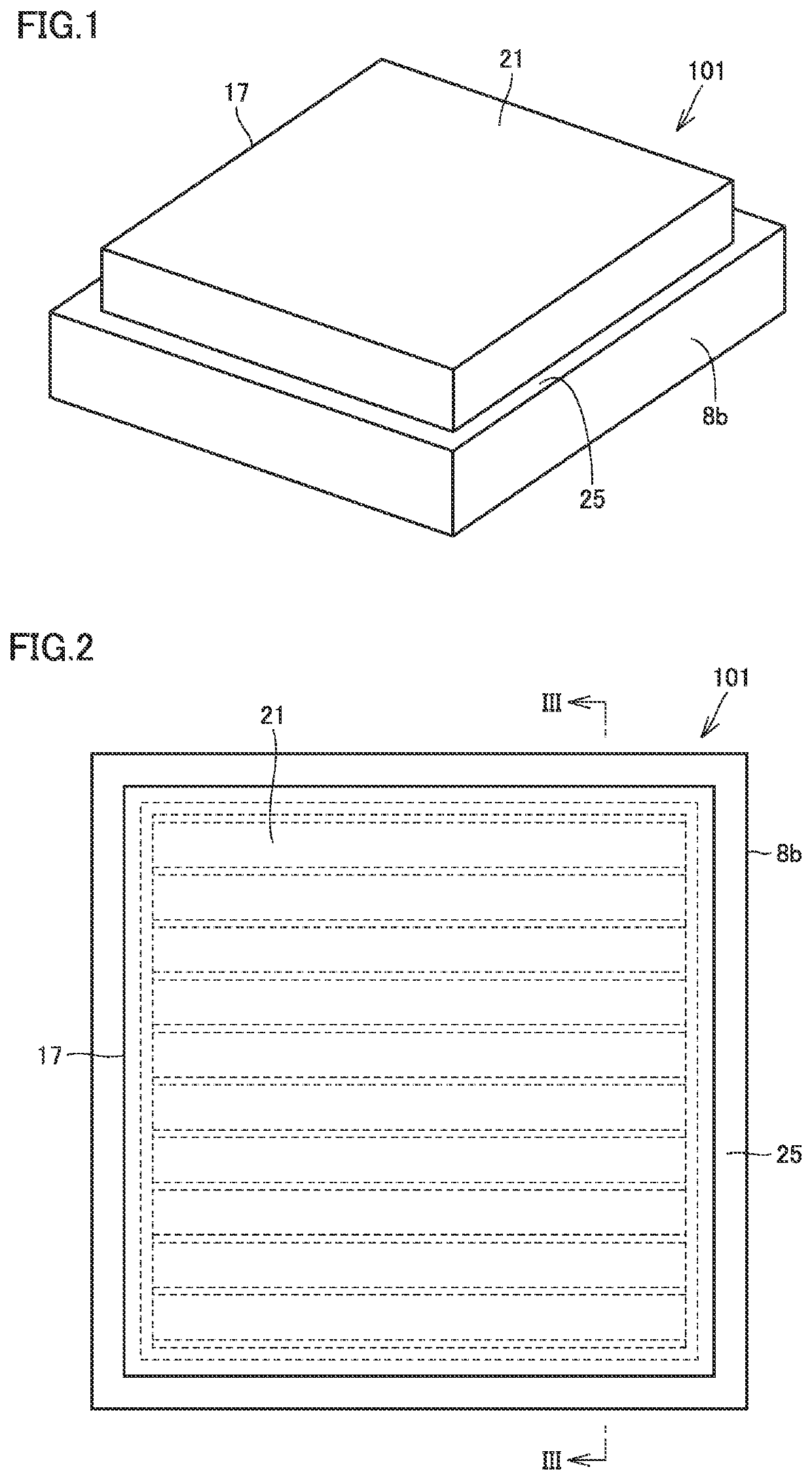
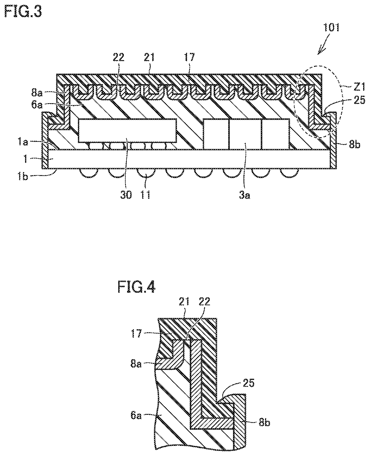
[0038]FIG. 1 shows an appearance of a module 101 in the present embodiment. Module 101 includes a resin protective layer 17. Module 101 includes a module upper surface 21. In the example shown here, module upper surface 21 is a wide flat surface in the center. Resin protective layer 17 is exposed at module upper surface 21. Module 101 includes a step portion 25 that surrounds an outer periphery. Module 101 includes a second shield film 8bthat covers side surfaces around the entire periphery. FIG. 2 shows a plan view of module 101. FIG. 3 shows a cross-sectional view along arrows III-III in FIG. 2. FIG. 4 shows an enlarged view of a Z1 portion in FIG. 3.

[0039]Module 101 includes a substrate 1 including a first main surface 1a, a first component 3a mounted on first main surface 1a, a first sealing resin 6a including a first upper surface 22, first component 3a being se...

second embodiment

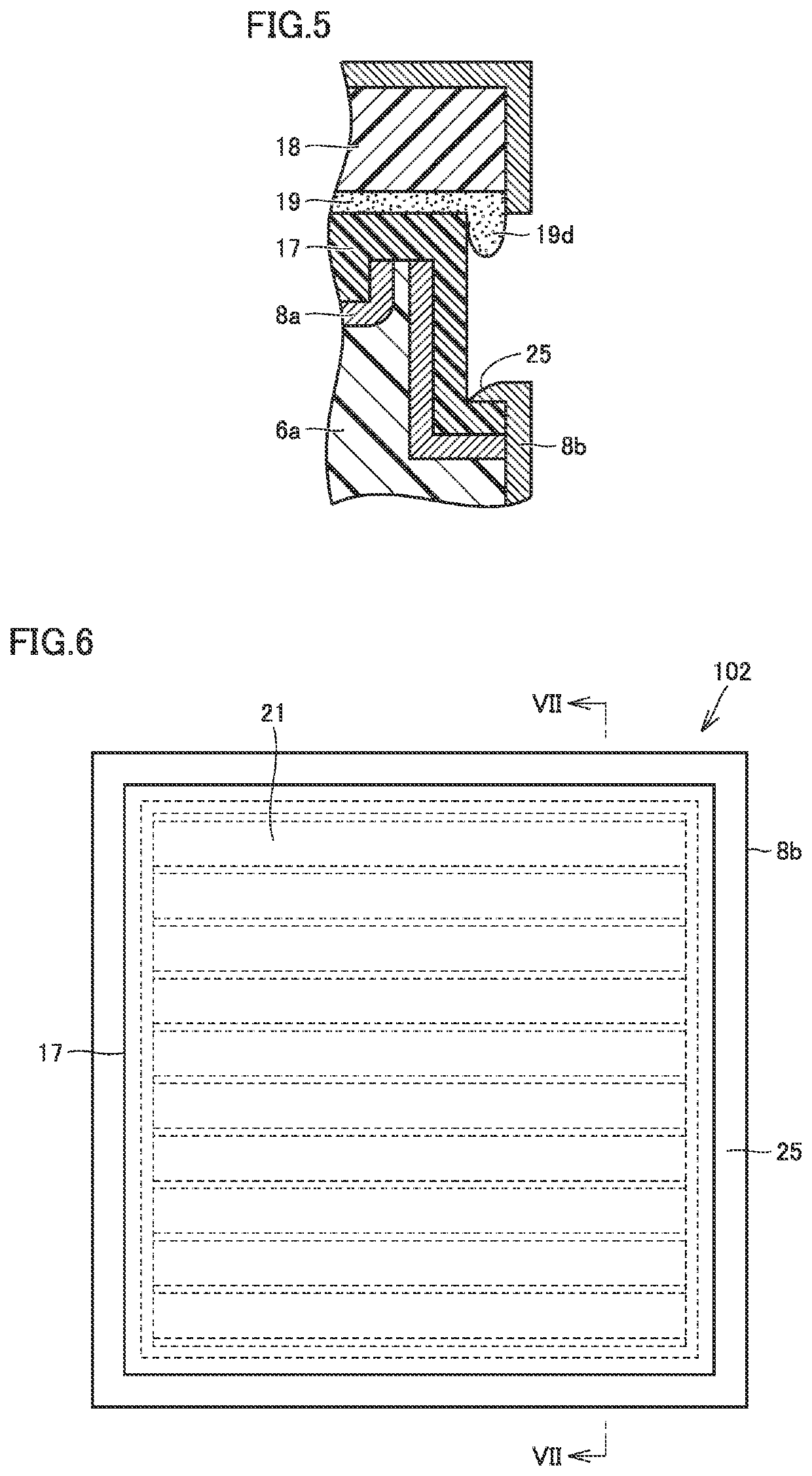
[0050]A module in a second embodiment based on the present disclosure will be described with reference to FIGS. 6 and 7. FIG. 6 shows a plan view of a module 102 in the present embodiment. FIG. 7 shows a cross-sectional view along arrows VII-VII in FIG. 6. Module 102 is similar in basic construction to module 101 described in the first embodiment. An enlarged view of a Z2 portion in FIG. 7 is the same as the enlarged view shown in FIG. 4.

[0051]In module 102, substrate 1 includes second main surface 1b on the side opposite to first main surface 1a. A second component 3b is mounted on second main surface 1b. A second sealing resin 6b is arranged to cover second main surface 1b and second component 3b. Second shield film 8bcovers a side surface of second sealing resin 6b. In other words, module 102 has what is called a double-sided mounting structure. A columnar conductor 13 is arranged on second main surface lb. Columnar conductor 13 passes through second sealing resin 6b in a directi...

third embodiment

[0053]A module in a third embodiment based on the present disclosure will be described with reference to FIGS. 8 and 9. FIG. 8 shows a plan view of a module 103 in the present embodiment. FIG. 9 shows a cross-sectional view along arrows IX-IX in FIG. 8. Module 103 is similar in basic construction to module 101 described in the first embodiment.

[0054]In module 103, first shield film 8a includes in first upper surface 22 of first sealing resin 6a, a portion 42 where a conductor film is formed all over. Portion 42 where the conductor film is formed all over is also called a solid-fill portion 42. Module 103 includes both of solid-fill portion 42 and a striped portion 41. Solid-fill portion 42 may be provided also in an area where generation of an eddy current does not have to be suppressed.

[0055]The “solid-fill portion” can also be expressed as a portion formed to two-dimensionally spread. The “solid-fill portion” may be in a rectangular shape or in another shape.

[0056]In the present e...


PUM

PropertyMeasurementUnit
forceaaaaaaaaaa
magnetic fieldaaaaaaaaaa
distanceaaaaaaaaaa

Abstract

A module includes a substrate including a first main surface, a first component mounted on the first main surface, a first sealing resin including a first upper surface, the first component being sealed with the first sealing resin, a first shield film that covers at least a part of the first upper surface of the first sealing resin, and a second shield film that covers a side surface of the first sealing resin and a side surface of the substrate. A step portion lower than the first upper surface of the first sealing resin is provided on an outer periphery of the first sealing resin. The first shield film and the second shield film are electrically connected to each other on a side surface below the step portion.

Description

CROSS REFERENCE TO RELATED APPLICATION[0001]This is a continuation of International Application No. PCT / JP2020 / 025794 filed on Jul. 1, 2020 which claims priority from Japanese Patent Application No. 2019-127017 filed on Jul. 8, 2019. The contents of these applications are incorporated herein by reference in their entireties.BACKGROUND OF THE DISCLOSUREField of the Disclosure[0002]The present disclosure relates to a module and a method of manufacturing the same.Description of the Related Art[0003]Japanese Patent Laying-Open No. 2012-9745 (PTL 1) describes a semiconductor device. In this semiconductor device, an electronic component is mounted on a substrate, and a sealing resin is formed on the substrate to seal the electronic component. A shield layer is formed in grids to cover a part of the sealing resin.[0004]PTL 1: Japanese Patent Laying-Open No. 2012-9745BRIEF SUMMARY OF THE DISCLOSURE[0005]In a module disclosed in PTL 1, an inductor may be employed as the electronic component....

Claims


Application Information

Patent Timeline
Patent Type & Authority Applications(United States)
IPC IPC(8): H01L23/552H01F41/00H01L25/16H01F27/36
CPCH01L23/552H01F27/363H01L25/16H01F41/005H05K9/00H01L23/28H01L23/00H01L25/50
Inventor KOMATSU, TORUNOMURA, TADASHI
Owner MURATA MFG CO LTD
Why Eureka
Try Eureka