LTPS TFT substrate structure and method of forming the same

Active Publication Date: 2016-12-06
TCL CHINA STAR OPTOELECTRONICS TECH CO LTD
View PDF2 Cites 0 Cited by
  • Summary
  • Abstract
  • Description
  • Claims
  • Application Information

AI Technical Summary

Benefits of technology

[0046]The present invention brings several benefits. The forming method of the LTPS TFT substrate of the present invention first defines the pattern of an a-Si layer with a photomask, expanding the chilled zone for crystallization so that the crystallization starts along the edge of the pattern and moves to the center of the pattern. Then, deposit and pattern a film of silicon oxide on the a-Si layer to produce a layer of silicon oxide on the a-Si layer in the display area. The silicon oxide layer serves as a photomask when the a-Si layer is annealed by excimer laser and crystallizes, and turns into a poly-Si layer. It forms relatively larger dies in the drive area and attains to higher electron mobility. The display ar

Problems solved by technology

The conventional forming method of the LTPS TFTs results in poorer uniformity in the display area, and lower-than

Method used


Image

  • LTPS TFT substrate structure and method of forming the same
  • LTPS TFT substrate structure and method of forming the same
  • LTPS TFT substrate structure and method of forming the same

Examples


Embodiment Construction

[0060]The drawings illustrate embodiments of the invention and, together with the description, serve to explain the principles of the invention.

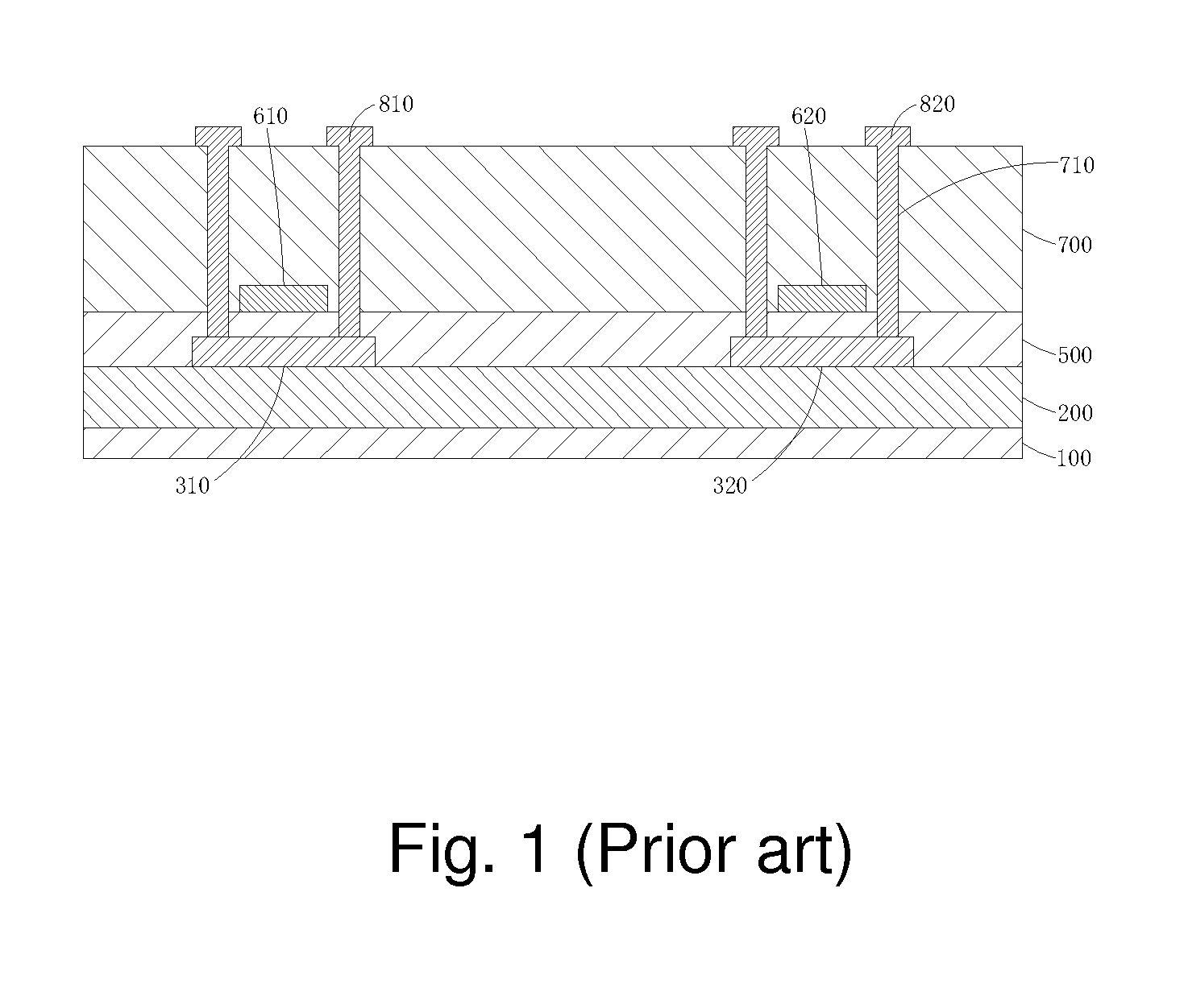
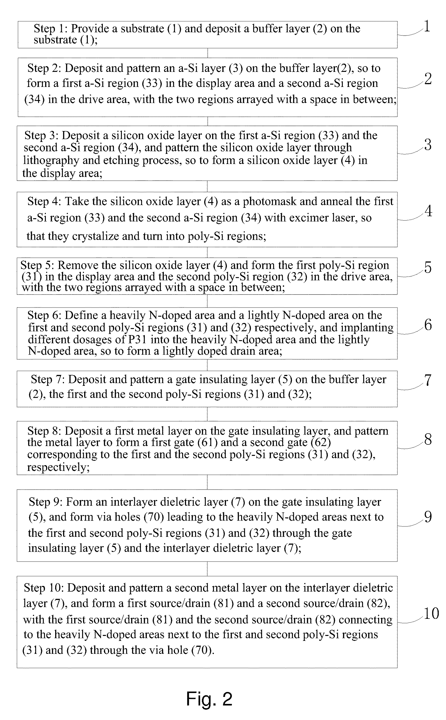
[0061]Please refer to FIG. 1. The present invention provides a method of forming a LTPS TFT substrate comprising the following steps:

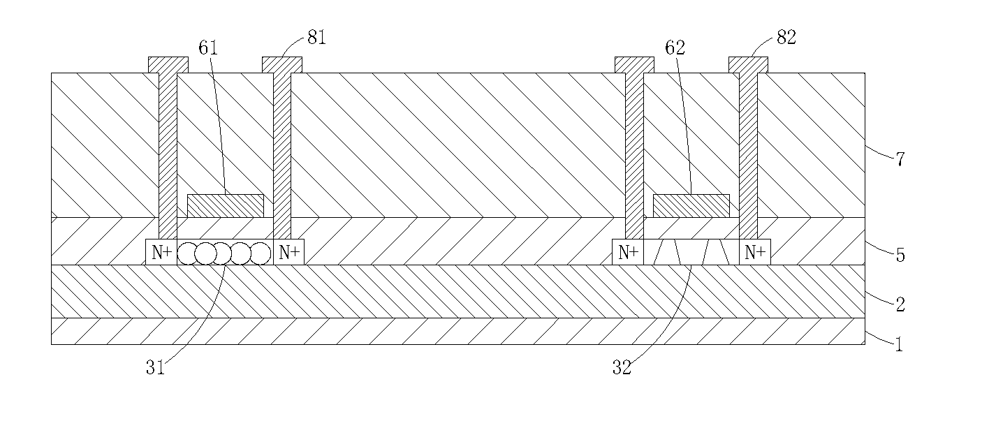
[0062]Step 1: Provide a substrate 1, and deposit a buffer layer 2 on the substrate 1, as shown in FIG. 3.

[0063]The substrate 1 is a transparent substrate which is made, preferably, of glass or plastic.

[0064]Specifically, the materials of the buffer layer 2 can be either silicon nitride (SiNx), silicon oxide (SiOx), or the combination of the two.

[0065]Step 2: As shown in FIGS. 4 and 5, deposit and pattern a first a-Si layer 3 on the buffer layer 2 to get a first a-Si region 33 in the display area and a second a-Si region 34 in the drive area. The two regions are arrayed with a space in between.

[0066]The step defines the pattern of the a-Si layer 3 with a photomask and etching, expanding the chilled zone for crys...


PUM


Abstract

A method of forming an LTPS TFT substrate includes: Step 1: providing a substrate (1) and depositing a buffer layer (2); Step 2: depositing an a-Si layer (3); Step 3: depositing and patterning a silicon oxide layer (4); Step 4: taking the silicon oxide layer (4) as a photomask and annealing the a-Si layer (3) with excimer laser, so that the a-Si layer crystallizes and turns into a poly-Si layer; Step 5: forming a first poly-Si region (31) and a second poly-Si region (32); Step 6: defining a heavily N-doped area and a lightly N-doped area on the first and second poly-Si regions (31) and (32), and forming an LDD area; Step 7: depositing and patterning a gate insulating layer (5); Step 8: forming a first gate (61) and a second gate (62); Step 9: forming via holes (70); and Step 10: forming a first source/drain (81) and a second source/drain (82).

Description

BACKGROUND OF THE INVENTION[0001]1. Field of the Invention[0002]The present invention relates to display technology, and more specifically, to a low temperature poly-silicon (LTPS) thin-film transistor (TFT) substrate structure and a method of forming the same.[0003]2. Description of the Prior Art[0004]Thin-film transistor liquid crystal display (TFT-LCD) can be achieved by two approaches: polycrystalline silicon (poly-Si) and amorphous silicon (a-Si). Low temperature poly-silicon (LTPS) is the latest generation of TFT-LCD producing technology. The biggest difference between a LTPS TFT-LCD and a conventional a-Si TFT-LCD is that the former responds faster, has higher brightness and resolution, and consumes less power.[0005]The crystalline silicons used by LTPS technology are arrayed more orderly than that used by a-Si technology. Therefore, the electron mobility of LTPS technology is over 100 times higher than that of a-Si technology. The peripheral driver can be built on the same g...

Claims


Application Information

Patent Timeline
IPC IPC(8): H01L27/12H01L29/786H01L29/49
CPCH01L27/1281H01L27/1222H01L27/1251H01L27/1274H01L27/1285H01L29/4908H01L29/78621H01L29/78675H01L29/66757
Inventor LU, GAIPING
Owner TCL CHINA STAR OPTOELECTRONICS TECH CO LTD
Why Eureka
Try Eureka