
Eureka
For R&D, Eureka makes reading and utilizing patents & technical documents easy.
Eureka AIR
Designed for self-driven R&D workflows. Generate viable solutions, solve complex R&D challenges, empower your innovation with AI.

Eureka Materials
Designed for material experts only. Revolutionize your material R&D, from search, analyze, to developing new materials.

TechResearch
Generate reliable direction feasibility study reports for your R&D in just a few steps.

TechSeek
Discover and master advanced knowledge NOW. Basics, ideas, possibilities, all at once.

TechMind
As an expert in R&D Theories, TechMind can generates customized viable solutions instantly.

TechRisk
Analyze your overall solution with one click, know your potential R&D risks in advance.

TechMonitor
Get weekly tech updates, stay abreast of the latest tech innovations and key insights.
Power conversion device
- Summary
- Abstract
- Description
- Claims
- Application Information
AI Technical Summary
Benefits of technology
Problems solved by technology
Method used
Image

Examples
embodiment 1
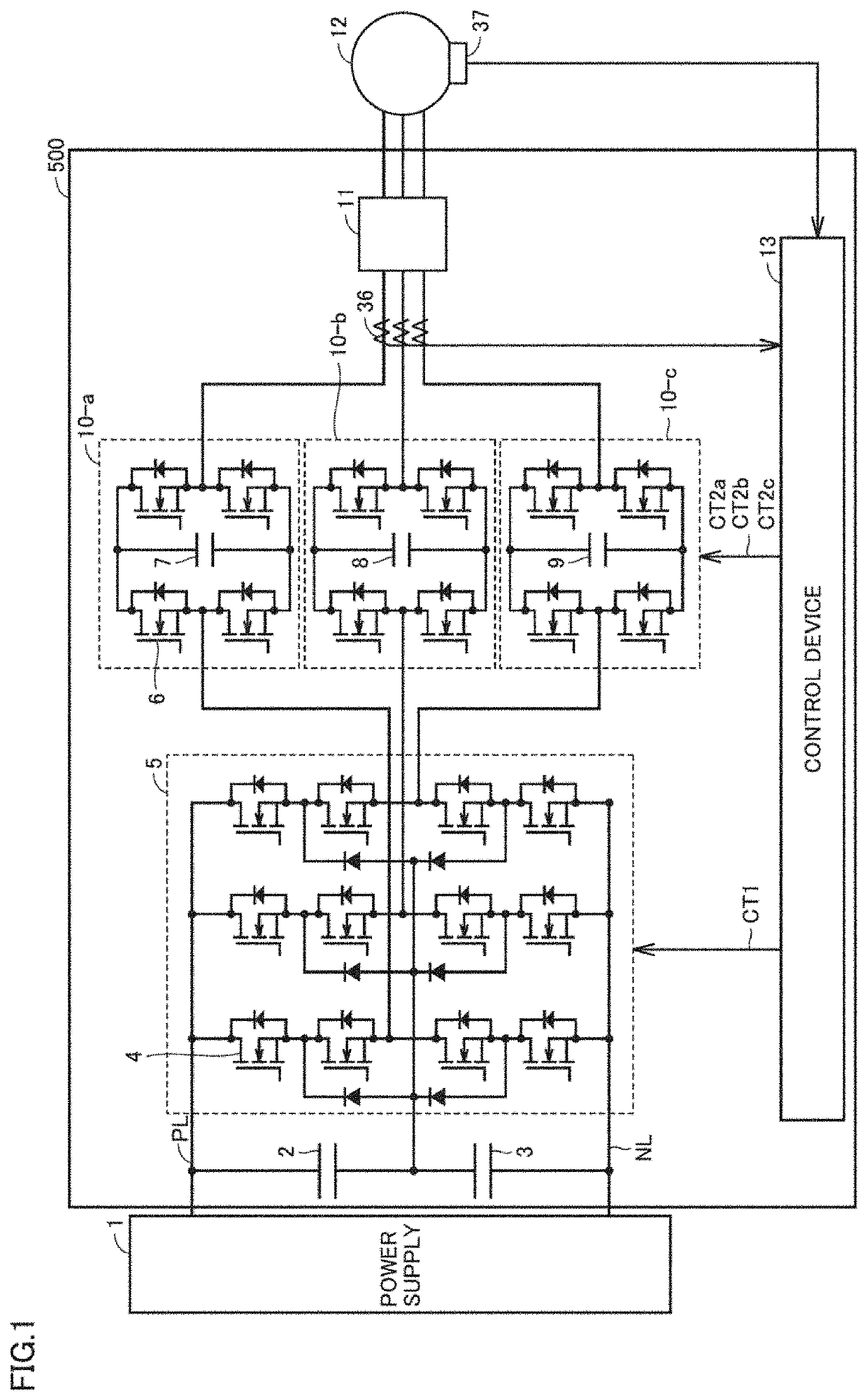
[0038]FIG. 1 is a diagram representing a configuration of a power conversion device 500 according to Embodiment 1.
[0039]Power conversion device 500 includes a first input capacitor 2, a second input capacitor 3, a three-phase three-level inverter 5, single-phase inverters 10, current sensors 36, an EMI noise filter 11, and a control device 13.
[0040]A direct-current power supply 1 corresponds to a first direct-current voltage source. A voltage of direct-current power supply 1 corresponds to a first voltage VM.
[0041]First input capacitor 2 and second input capacitor 3 are connected in series between a positive busbar PL and a negative busbar NL. First input capacitor 2 and second input capacitor 3 divide first voltage VM of direct-current power supply 1.
[0042]Three-phase three-level inverter 5 includes multiple switching elements 4 and multiple diodes. Switching element 4 is, for example, a Si-IGBT (Insulated Gate Bipolar Transistor), a Si-MOSFET (Metal Oxide Semiconductor Field Effec...
embodiments 2
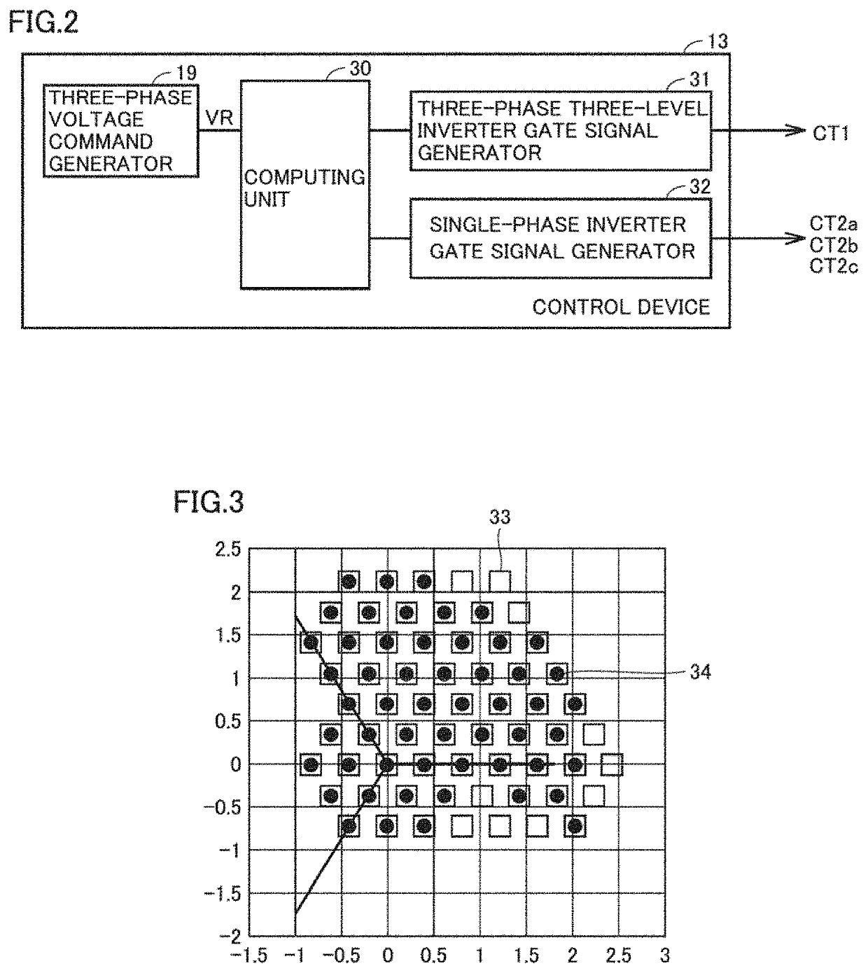
[0073]A power conversion device 500 according to Embodiments 2 is the same as power conversion device 500 according to Embodiment 1, except for the processing content of a computing unit 30 included in a control device 13.
[0074]In the present embodiment, a computing unit 30 selects vectors of combined output voltages CVa, CVb, and CVc so that a “first condition” (=common mode voltage Vcom3 of combined output voltages CVa, CVb, and CVc is within a predetermined range”) and a “second condition” (the variation ranges of line voltages DVab, DVbc, and DVca between combined output voltages CVa, CVb, and CVc is a specified condition established with a second voltage Vs as a reference) are satisfied, as with Embodiment 1.
[0075]In the present embodiment, the first condition is that “common mode voltage Vcom3 of combined output voltages CVa, CVb, and CVc is suppressed to 0V, and the “second condition” is that “the variation ranges of line voltages DVab, DVbc, and DVca between combined output ...
embodiment 3
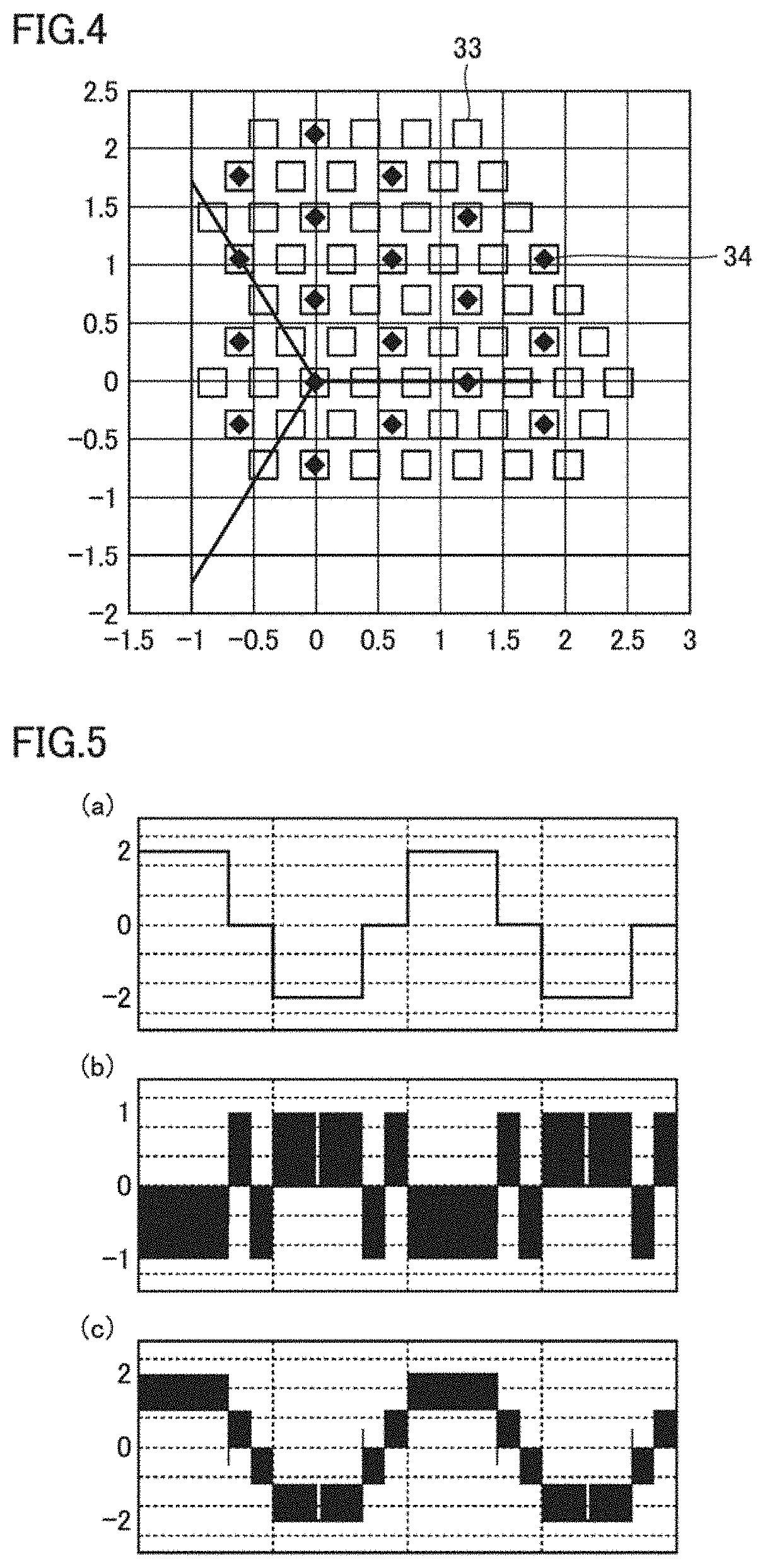
[0085]A power conversion device 500 according to Embodiment 3 is a refinement of power conversion device 500 according to Embodiment 1.
[0086]In Embodiment 3, computing unit 30 adjusts a common mode voltage Vcom3 of combined output voltages CVa, CVb, and CVc to be suppressed to ⅔ or below a second voltage Vs, and the variation ranges of line voltages DVab, DVbc, and DVca between combined output voltages CVa, CVb, and CVc to be suppressed to second voltage Vs or below, as with Embodiment 1.
[0087]Part (a) of FIG. 5 is a diagram representing a U-phase output voltage V_a of a three-phase three-level inverter 5. Part (b) of FIG. 5 is a diagram representing a boost voltage TVa generated by a single-phase inverter 10-a. Part (c) of FIG. 5 is a diagram representing a combined output voltage CVa.
[0088]As shown in (a) of FIG. 5, three-phase three-level inverter 5 outputs a voltage to be the fundamental wave of a load 12, such as an square wave output of one pulse, and supplies the real power t...
PUM
 Abstract
Description
Claims
Application Information
 - R&D Engineer
- R&D Manager
- IP Professional
- Industry Leading Data Capabilities
- Powerful AI technology
- Patent DNA Extraction
Browse by: Latest US Patents, China's latest patents, Technical Efficacy Thesaurus, Application Domain, Technology Topic, Popular Technical Reports.
© 2024 PatSnap. All rights reserved.Legal|Privacy policy|Modern Slavery Act Transparency Statement|Sitemap|About US| Contact US: help@patsnap.com