Notch detecting method

Pending Publication Date: 2022-05-05
DISCO CORP
View PDF0 Cites 0 Cited by
  • Summary
  • Abstract
  • Description
  • Claims
  • Application Information

AI Technical Summary

Benefits of technology

The present invention relates to a method of detecting a notch in a wafer. The method can determine if an irregularly shaped area in the outer edge of the wafer is a notch or not, based on its size or shape. This helps to prevent mistakenly identifying other indents in the wafer as notches, and ensures proper detection of the notch.

Problems solved by technology

For example, when such a notched wafer is machined in a cutting process, a grinding process, or the like, if the machining tool contacts the wafer, it may chip a fragment off from the outer circumferential portion of the wafer, forming an unintentional indentation therein that appears to be similar to the notch.
In the presence of the indentation, a subsequent process of detecting the notch of the wafer may tend to fail to identify the notch or the indentation correctly, i.e., may determine the accidentally formed indentation as the notch in error.
As a result, the wafer is processed while being directed in a wrong orientation, and is liable to suffer a processing failure.

Method used


Image

  • Notch detecting method
  • Notch detecting method
  • Notch detecting method

Examples


Embodiment Construction

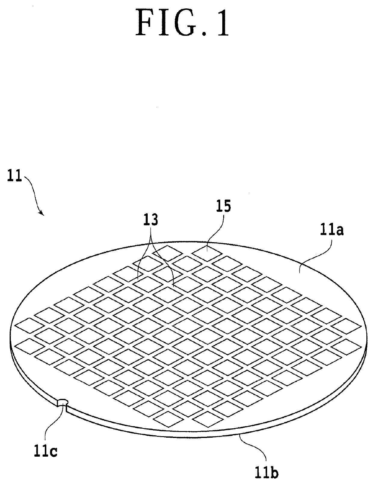
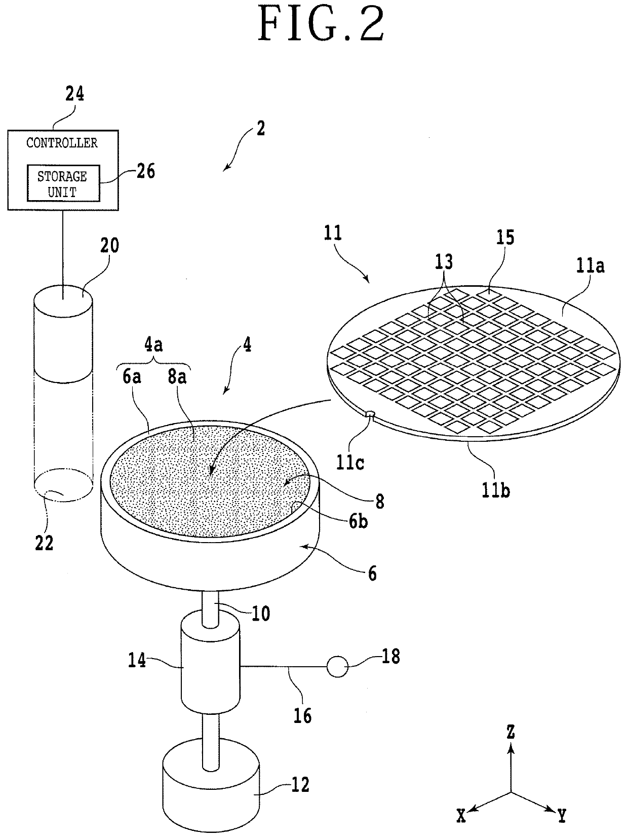
[0031]A notch detecting method according to a preferred embodiment of the present invention will be described hereinbelow with reference to the accompanying drawings. First, a wafer whose notch is to be detected by the notch detecting method according to the present embodiment will be described below. FIG. 1 illustrates the wafer, generally denoted by 11, in perspective.

[0032]The wafer 11 is a disk-shaped crystalline wafer made of a semiconductor such as silicon, for example, and includes a face side 11a and a reverse side 11b lying generally parallel to each other. The wafer 11 has a plurality of rectangular areas demarcated on the face side 11a by a grid of intersecting streets or projected dicing lines 13. Devices 15 such as integrated circuits (ICs), large-scale integration (LSI) circuits, light-emitting diodes (LEDs), or microelectromechanical systems (MEMSs) are formed respectively in the rectangular areas demarcated on the face side 11a by the streets 13.

[0033]The wafer 11 ha...


PUM


Abstract

A notch detecting method for detecting a notch defined in an outer circumferential portion of a wafer includes a placing step of placing the wafer on a rotary table, an image capturing step of acquiring an image of the outer circumferential portion of the wafer, a contour data acquiring step of acquiring contour data including coordinates of a contour of the wafer, a hypothetical circle calculating step of calculating a hypothetical circle that approximates the contour of the wafer, an irregularly shaped area determining step of determining whether an irregularly shaped area exists in the outer circumferential portion of the wafer or not, and a first notch determining step of determining whether the irregularly shaped area is the notch or not.

Description

BACKGROUND OF THE INVENTIONField of the Invention[0001]The present invention relates to a notch detecting method for detecting a notch representing a crystal orientation of a wafer.Description of the Related Art[0002]Device chip manufacturing processes produce device chips by processing wafers where devices are formed in respective areas demarcated on the wafers by a grid of streets, also known as projected dicing lines, established on face sides of the wafers. The wafers are divided along the streets into a plurality of device chips having the respective devices. The device chips thus fabricated will be used in various electronic appliances including mobile phones, personal computers, etc.[0003]A wafer is divided by a cutting apparatus, for example. The cutting apparatus divides the wafer, i.e., a workpiece, by causing a rotating annular cutting blade to cut into the wafer. A wafer may alternatively be divided by a laser processing apparatus that includes a laser beam applying unit...

Claims


Application Information

Patent Timeline
IPC IPC(8): G06T7/00G06T7/13G01B11/24
CPCG06T7/001G06T7/13G06T2207/20021G06T2207/30148G01B11/24H01L22/12H01L22/26H01L21/68H01L21/683H01L21/6838H01L21/68714H01L21/68785H01L21/68792G06T7/73H01L21/67259H01L23/544H01L2223/54493
Inventor NOMURA, YASUKUNIYOSHIDA, SHINJI
Owner DISCO CORP
Why Eureka
Try Eureka