SiC EPITAXIAL WAFER AND METHOD FOR PRODUCING SiC EPITAXIAL WAFER

Active Publication Date: 2022-06-02
SHOWA DENKO KK
View PDF2 Cites 0 Cited by
  • Summary
  • Abstract
  • Description
  • Claims
  • Application Information

AI Technical Summary

Benefits of technology

The present invention provides a SiC epitaxial wafer and a method for producing it, which controls the density and distribution of a specific point and prevents device deterioration when used as a device.

Problems solved by technology

However, at the time of production, there are a plurality of parameters which affect a density and a distribution of Z1 / 2 centers and it is difficult to control each of these parameters.

Method used


Image

  • SiC EPITAXIAL WAFER AND METHOD FOR PRODUCING SiC EPITAXIAL WAFER
  • SiC EPITAXIAL WAFER AND METHOD FOR PRODUCING SiC EPITAXIAL WAFER
  • SiC EPITAXIAL WAFER AND METHOD FOR PRODUCING SiC EPITAXIAL WAFER

Examples


example 1

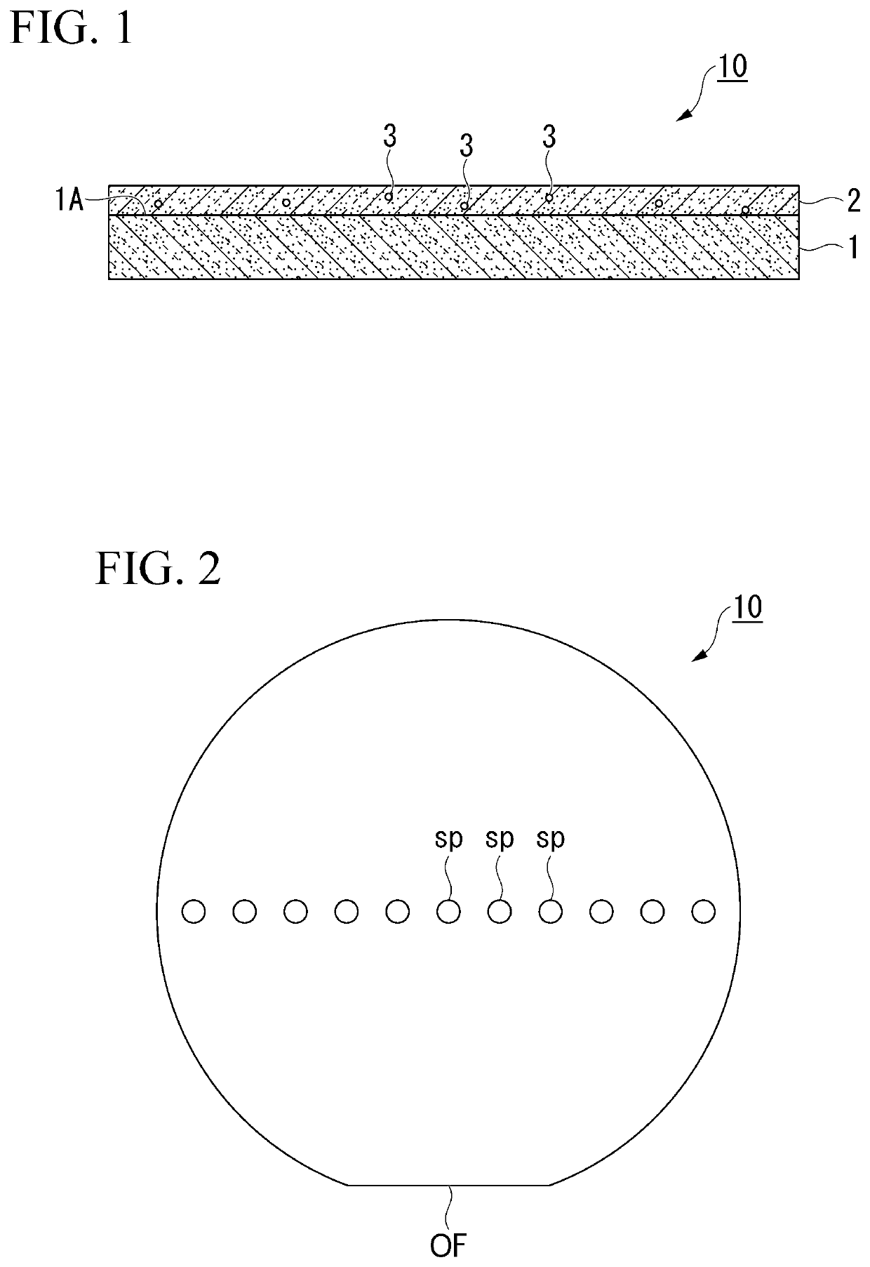
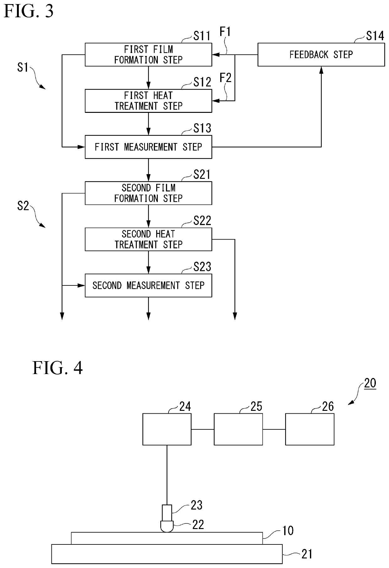
[0082]The test step S1 described above was repeatedly performed a plurality of times to determine the optimum conditions for film formation and heat treatment. Moreover, as the main step S2, a SiC epitaxial layer with a thickness of 16 μm was formed on a 4H-SiC substrate with a diameter of 150 mm. A doping concentration and a Z1 / 2 center density of the SiC epitaxial layer were obtained in the non-destructive manner shown in FIG. 4. Measurement points were measured in a cross shape at a pitch of 10 mm within a range of a radius of 50 mm from a center of the SiC substrate. The Z1 / 2 center density was obtained from a measurement value of the doping concentration at each of the measurement points. FIG. 6 shows the Z1 / 2 center density and the doping concentration at each of the measurement points in Example 1. In FIG. 6, Nd is a donor concentration and Na is an acceptor concentration.

[0083]As shown in FIG. 6, the Z1 / 2 center density and the doping concentration were uniform in the in-pla...


PUM


Abstract

A SiC epitaxial wafer according to an embodiment includes: a SiC substrate; and a SiC epitaxial layer formed on a first surface of the SiC substrate. The in-plane uniformity of a density of Z1 / 2 centers of the SiC epitaxial layer is 5% or less.

Description

BACKGROUND OF THE INVENTIONField of the Invention[0001]The present invention relates to a SiC epitaxial wafer and a method for producing a SiC epitaxial wafer.[0002]Priority is claimed on Japanese Patent Application No. 2020-199012, filed Nov. 30, 2020, the content of which is incorporated herein by reference.Description of Related Art[0003]Silicon carbide (SiC) has an insulation breakdown electric field which is an order of magnitude larger than that of silicon (Si) and a band gap which is three times larger than that of silicon (Si). Furthermore, silicon carbide (SiC) has characteristics such as a thermal conductivity which is about three times higher than that of silicon (Si). For this reason, silicon carbide (SiC) is expected to be applied to power devices, high frequency devices, high temperature operation device, and the like. For this reason, in recent years, SiC epitaxial wafers have been used for the semiconductor devices as described above.[0004]SiC epitaxial wafers are ob...

Claims


Application Information

Patent Timeline
IPC IPC(8): H01L21/66H01L21/02
CPCH01L22/20H01L21/02529H01L21/02378H01L21/02664H01L21/02634C30B29/36H01L22/12C23C16/325
Inventor ISHIBASHI, NAOTOMURATA, KOICHITSUCHIDA, HIDEKAZU
Owner SHOWA DENKO KK
Why Eureka
Try Eureka