
Contact and socket device for burning-in and testing semiconductor IC

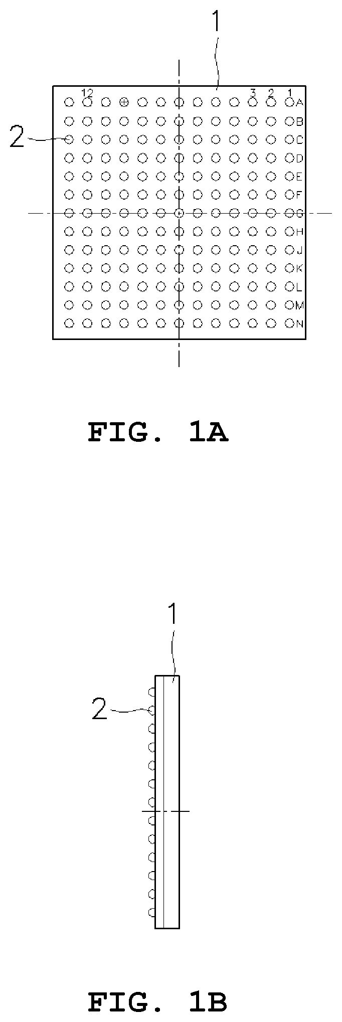
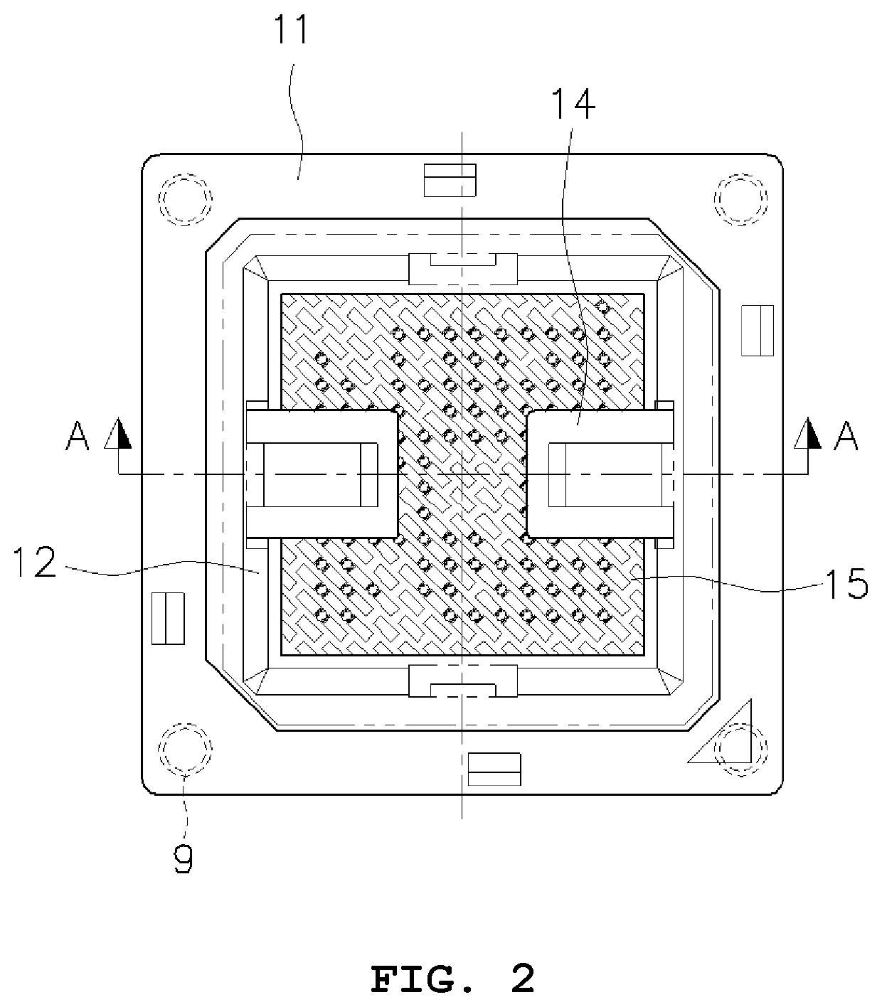
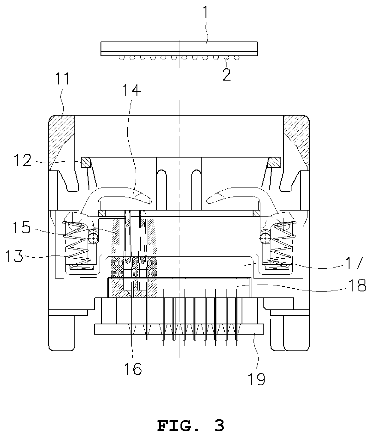
a socket device and contact technology, applied in semiconductor/solid-state device testing/measurement, semiconductor operation lifetime testing, instruments, etc., can solve the problems of high manufacturing cost, high assembly time, and inefficient air flow, so as to reduce the height reduce the size of the socket device, and increase space efficiency

Active Publication Date: 2022-06-23
HICON CO LTD +3
View PDF2 Cites 0 Cited by
  • Summary
  • Abstract
  • Description
  • Claims
  • Application Information

AI Technical Summary

Benefits of technology

The present invention is a lidless socket device that removes a cover, making it smaller and flatter than conventional devices. It allows for more efficient space inside test equipment, resulting in faster testing. The contact length is shorter, enabling higher speeds. The top surface of the IC is exposed, allowing for direct control of temperature. Additionally, the invention allows for testing the top surface of the IC by pressing it. This can be useful in future applications such as artificial intelligence and driverless cars.

Problems solved by technology

1. Overall, there are many complicated components, so it takes much assembly time and manufacturing cost is high.
2. When the IC is loaded, the IC guide or the cover surrounds the IC, so an air flow is not efficient and heat generated by the IC is not effectively discharged to surroundings.
3. The height of the socket including the cover that is manipulated up and down from the top of the socket is high, and the entire height of a burn-in board is high. Accordingly, when it is required that inside a burn-in chamber, several burn-in boards are arranged in a vertical direction and appropriate air between the burn-in boards flows, the number of the burn-in boards which can be arranged is decreased.
4. The forced flow of air generated in the burn-in chamber is obstructed by the cover or the IC guide, which is a part of the socket, and the air is not effectively transmitted to the surface of the IC. Accordingly, it is difficult to maintain the even temperature of the IC.
5. In the pinch type contact, the contact or release of the contact with the ball terminal is performed by horizontal manipulation of the movable terminal. In this case, the movable terminal undergoes repetitive elastic deformation, and a contact force of the contact with the ball terminal decreases due to decrease in durability due to repeated use. Particularly, in the BGA socket device of the conventional technology, in the process of restoring the movable terminal (see FIG. 5C), the restoration of the slider to an initial position is performed by the elastic restoring force of the movable terminal. Accordingly, as the number of uses of the movable terminal increases, the elastic restoring force of the movable terminal gradually decreases due to the stress of the movable terminal. Accordingly, the contact force of the contact with the ball terminal is decreased, which leads to decrease in the reliability of the test of the IC.

Method used


Image

  • Contact and socket device for burning-in and testing semiconductor IC
  • Contact and socket device for burning-in and testing semiconductor IC
  • Contact and socket device for burning-in and testing semiconductor IC

Examples


first embodiment

[0102]FIG. 6 is a top plan view of a socket device according to the present disclosure; FIG. 7 is a sectional view taken along line B-B of FIG. 6; and FIG. 8 is a cross-sectional view taken along line C-C of FIG. 6.

[0103]Referring to FIGS. 6 to 8, the socket device 200 for testing a semiconductor IC according to the embodiment includes: contacts 110; a main body part 210 having first receiving holes 211 formed therein and a plurality of mounting parts 212 fixed to a PCB, wherein each of the first receiving holes allows an upper end of each of the contacts 110 to be inserted therethrough and allows the contact to be compressed and moved downward; a lower plate 220 assembled with a lower end of the main body part 210 and having a second receiving hole 221 formed at a position corresponding to the first receiving hole 211, the second receiving hole allowing a lower terminal part 122 of the contact 110 to be inserted therethrough; a floating plate 230 having a contact hole 231 formed at...

third embodiment

[0130]FIG. 14 is a perspective view of the contact according to the present disclosure.

[0131]Referring to FIG. 14, a contact 130 of the third embodiment is composed of an upper terminal part 131; a lower terminal part 132; and an elastic part 133a and 133b, and is substantially the same as the contact of the first embodiment. Particularly, the upper terminal part 131 may be formed to have a cylindrical shape by rolling and bending the plate, and includes an upper tip part 131b having a plurality of contact points configured as a crown shape formed by pointedly protruding along the circumference of the upper end part of the upper terminal part.

[0132]Meanwhile, in the embodiment, only the upper terminal part is illustrated to have a cylindrical shape, but the lower terminal part may be also configured to have a cylindrical shape according to the shape of the terminal (a pad) of the PCB.

[0133]FIG. 15 is a perspective view of a contact according to a fourth embodiment of the present dis...

fifth embodiment

[0136]Referring to FIGS. 16A, 16B, and 16C, a contact 150 of the fifth embodiment includes an upper terminal part 151 having an upper tip part 151b at an upper end part thereof; a lower terminal part 152 having a lower tip part 152b at a lower end part thereof and being assembled with the upper terminal part 151 by crossing each other in a longitudinal direction of the contact; and a spring 153 fitted over the upper terminal part 151 and the lower terminal part 152 therebetween and elastically supporting the upper terminal part 151 and the lower terminal part 152.

[0137]Each of the upper terminal part 151 and the lower terminal part 152 has the same shape, and is formed to have a thickness of a plate in a longitudinal direction thereof. The upper terminal part 151 and the lower terminal part 152 have a first slot 151c and a second slot 152c, respectively, formed therein, and are inserted into the spring 153 by crossing each other by 90° to be assembled with each other.

[0138]As illust...


PUM

PropertyMeasurementUnit
widthaaaaaaaaaa
thicknessaaaaaaaaaa
elasticaaaaaaaaaa

Abstract

A contact for burning-in and testing a semiconductor IC and a socket device including the contact are proposed. The contact includes: an upper terminal part (111) having an upper tip part (111b) at an upper end part thereof; a lower terminal part (112) having a lower tip part (112c) at a lower end part thereof and provided on the same axis as the upper terminal part (111); and an elastic part (113) elastically supporting the upper terminal part (111) and the lower terminal part (112), wherein the upper terminal part (111) and the lower terminal part (112) include a shoulder part (111a) and a shoulder part (112a), respectively, formed by protruding therefrom in width directions thereof, and the elastic part (113) has a third width (w3), and includes a first strip (113a) and a second strip (113b).

Description

CROSS REFERENCE TO RELATED APPLICATION[0001]The present application claims priority to Korean Patent Application No. 10-2020-0178794, filed Dec. 18, 2020, the entire contents of which is incorporated herein for all purposes by this reference.BACKGROUND OF THE INVENTIONField of the Invention[0002]The present disclosure relates to a contact and a socket device for burning-in and testing a semiconductor IC.Description of the Related Art[0003]Generally, a socket device for testing a semiconductor device (an integrated circuit, IC) (hereinafter, referred to as IC) is provided on a test board or a burn-in board. The socket device allows a burn-in chamber or a peripheral device thereof inputting and outputting power having a predetermined voltage and electrical signals required for driving the IC and separate test devices for measuring characteristics of the IC to be connected to each other by the input and output terminals of the board, and thus is used in a system for testing the IC.[000...

Claims


Application Information

Patent Timeline
Patent Type & Authority Applications(United States)
IPC IPC(8): G01R31/28H01L21/66
CPCG01R31/2863H01L22/14G01R31/2879G01R31/2865G01R1/0466G01R31/2642G01R31/2886
Inventor HWANG, DONG WEONHWANG, LOGAN JAEHWANG, JAE BAEK
Owner HICON CO LTD
Learn More