Check patentability & draft patents in minutes with Patsnap Eureka AI!

Wafer inspection method

a wafer and inspection method technology, applied in the direction of image enhancement, semiconductor/solid-state device testing/measurement, instruments, etc., can solve the problems of requiring a considerable amount of time and cost to transfer the wafer to the ebr inspection apparatus

Pending Publication Date: 2022-06-30
SEMES CO LTD
View PDF0 Cites 0 Cited by
  • Summary
  • Abstract
  • Description
  • Claims
  • Application Information

AI Technical Summary

Benefits of technology

The present invention provides a way to inspect wafers faster and more cost-effectively, while also making the inspection results more reliable.

Problems solved by technology

Accordingly, a considerable amount of time and cost may be required to transfer the wafer to the EBR inspection apparatus and to perform the EBR inspection process using the EBR inspection apparatus.

Method used


Image

  • Wafer inspection method
  • Wafer inspection method
  • Wafer inspection method

Examples


Embodiment Construction

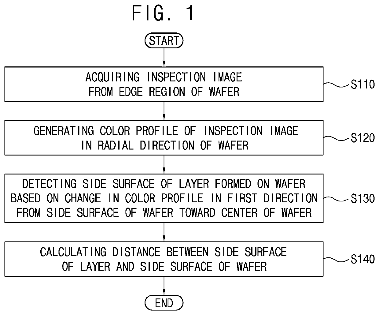
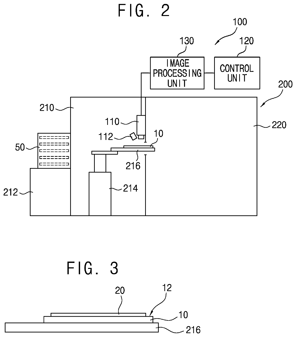
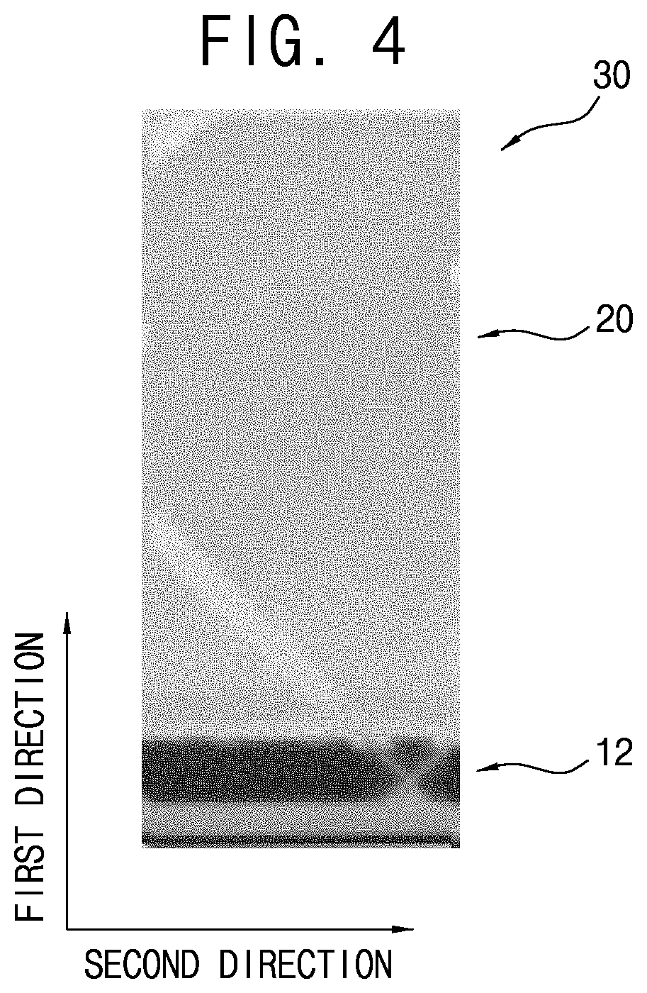
[0040]Hereinafter, embodiments of the present invention are described in more detail with reference to the accompanying drawings. However, the present invention is not limited to the embodiments described below and is implemented in various other forms. Embodiments below are not provided to fully complete the present invention but rather are provided to fully convey the range of the present invention to those skilled in the art.

[0041]In the specification, when one component is referred to as being on or connected to another component or layer, it can be directly on or connected to the other component or layer, or an intervening component or layer may also be present. Unlike this, it will be understood that when one component is referred to as directly being on or directly connected to another component or layer, it means that no intervening component is present. Also, though terms like a first, a second, and a third are used to describe various regions and layers in various embodime...


PUM


Abstract

A wafer inspection method includes acquiring an inspection image from an edge region of a wafer, generating a color profile of the inspection image in a radial direction of the wafer, detecting a side surface of a layer formed on the wafer based on a change in the color profile in a first direction from a side surface of the wafer toward a center of the wafer, and calculating a distance between the side surface of the layer and the side surface of the wafer.

Description

CROSS-REFERENCE TO RELATED APPLICATION[0001]This application claims the priority benefit of Korean Patent Application No. 10-2020-0184881, filed on Dec. 28, 2020, and all the benefits accruing therefrom under 35 U.S.C. § 119, the contents of which are incorporated by reference in their entirety.TECHNICAL FIELD[0002]The present disclosure relates to a wafer inspection method. More specifically, the present disclosure relates to a wafer inspection method of inspecting a distance between a side surface of a wafer and a side surface of a layer formed on the wafer.BACKGROUND[0003]Semiconductor devices may be formed on a substrate such as a silicon wafer by repeatedly performing a series of manufacturing processes. For example, a deposition process may be performed to form a layer on the wafer, a photolithography process may be performed to form a photoresist pattern on the layer, an etching process may be performed to pattern the layer formed on the wafer by using the photoresist pattern...

Claims


Application Information

Patent Timeline
IPC IPC(8): H01L21/67G06T7/90G06T7/70G06T7/11G06T7/00
CPCH01L21/67288G06T7/90G06T7/70G06T2207/30148G06T7/0004G06T2207/10024G06T7/11H01L22/24H01L22/12H01L22/20H01L21/67259G01N21/8851G01N21/9503G06T2210/36
Inventor WOO, MYOUNG HOON
Owner SEMES CO LTD
Features
  • R&D
  • Intellectual Property
  • Life Sciences
  • Materials
  • Tech Scout
  • Unparalleled Data Quality
  • Higher Quality Content
  • 60% Fewer Hallucinations
Learn More