Switching power supply, power adapter and charger
- Summary
- Abstract
- Description
- Claims
- Application Information
AI Technical Summary
Benefits of technology
Problems solved by technology
Method used
Image
Examples
Embodiment Construction
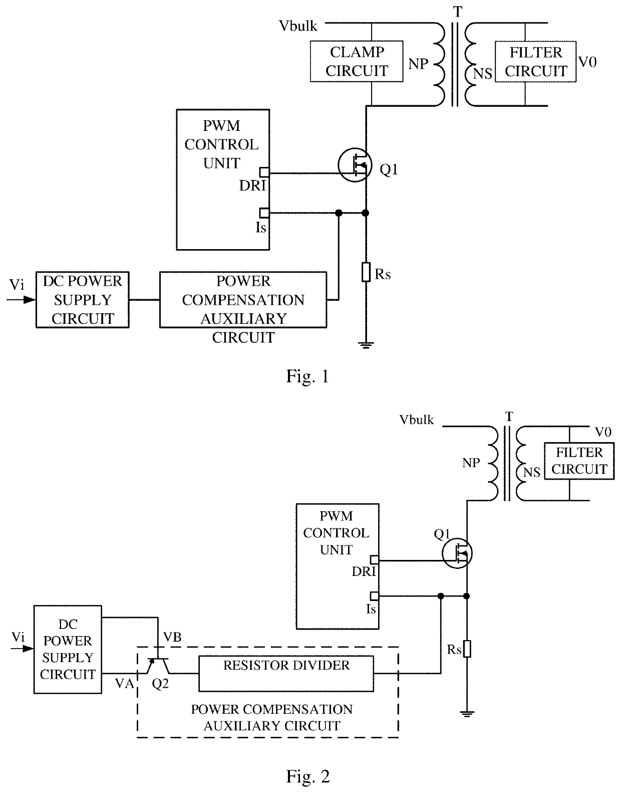
[0044]FIG. 1 is a schematic diagram of a switching power supply according to one embodiment of the invention. The switching power supply has a wide output voltage range, i.e. a wide output voltage range, such as 2-30V, or 5-24V, or a variable output voltage (5V-9V / 5V-11V / 5V-12V / 5V-15V / 5V-20V), or its output voltage range Vmin-Vmax overlaps at least partially with the voltage range of 5-24V. The switching power supply is especially suitable for fast charging power adapters or chargers with high power density and wide output voltage.
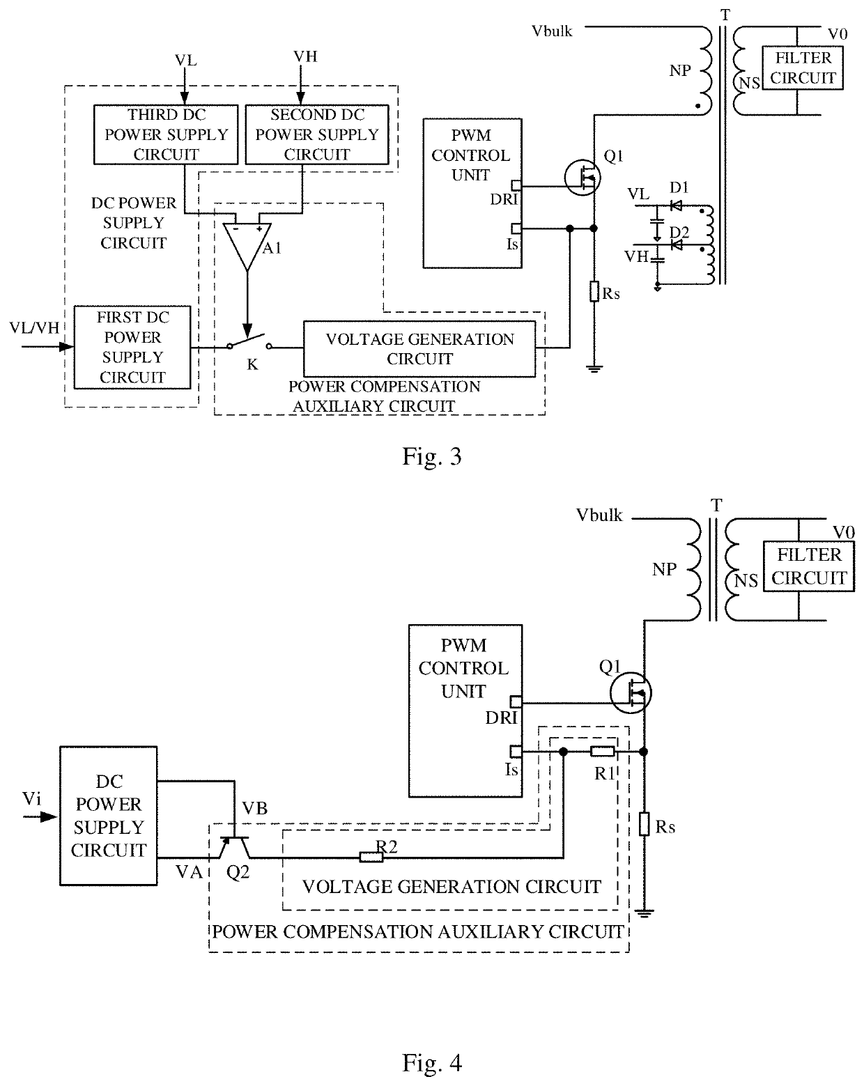
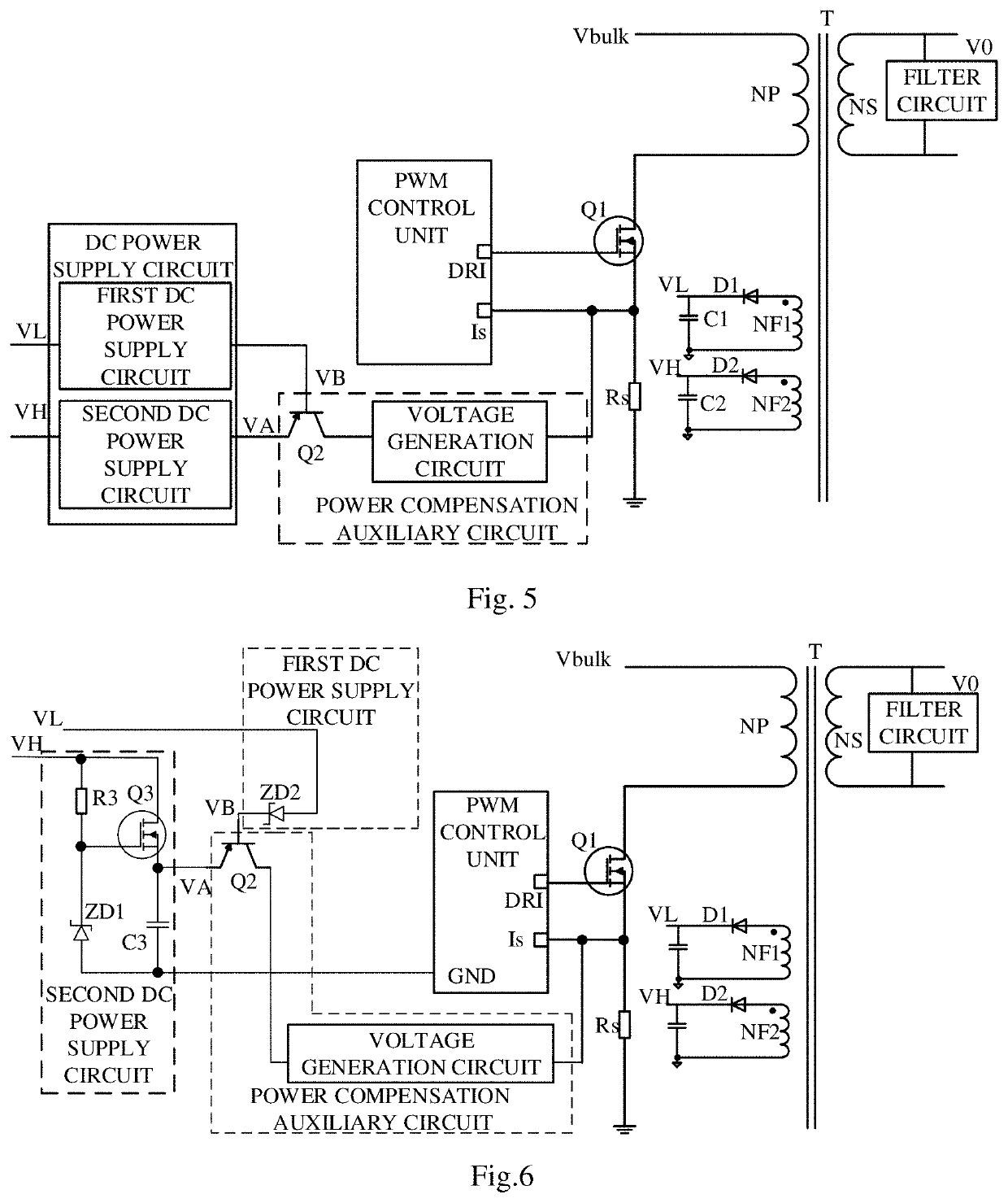
[0045]The switching power supply comprises a current-mode PWM control unit (e.g., a current-mode PWM control chip), a transformer T, a power switch transistor Q1, a current sampling resistor Rs, a DC power supply circuit, a power compensation auxiliary circuit, a clamp circuit, a filter circuit, and a voltage feedback circuit (not shown in the figure). The primary winding NP of the transformer T is fed with a rectified DC voltage Vbulk (the DC voltage Vbul...
PUM
 Abstract
Description
Claims
Application Information
 - R&D
- Intellectual Property
- Life Sciences
- Materials
- Tech Scout
- Unparalleled Data Quality
- Higher Quality Content
- 60% Fewer Hallucinations
Browse by: Latest US Patents, China's latest patents, Technical Efficacy Thesaurus, Application Domain, Technology Topic, Popular Technical Reports.
© 2025 PatSnap. All rights reserved.Legal|Privacy policy|Modern Slavery Act Transparency Statement|Sitemap|About US| Contact US: help@patsnap.com


