Electronic device and method for producing the same

Pending Publication Date: 2022-07-28
SHIN-ETSU HANDOTAI CO LTD
View PDF0 Cites 0 Cited by
  • Summary
  • Abstract
  • Description
  • Claims
  • Application Information

AI Technical Summary

Benefits of technology

This patent method and device can make solar cells with a diode circuit and capacitor function in a smaller area, reducing production costs.

Problems solved by technology

However, mounting cost required for wiring becomes massive, and inexpensive sensor-mounting becomes difficult.
However, microwaves have great output attenuation due to distance, and are not suitable as an electricity supply system for sensors for IoT having a dispersal arrangement.
A power receiving device for optical wireless power receiving is a solar cell, and it is difficult to provide a drive circuit and a power receiving device in one chip.
However, the power receiving efficiency of a Si-based solar cell on which a drive circuit is mounted is not high, and a large area is required.
As a result, it is difficult to fabricate an inexpensive device.
However, if epitaxial growth of a compound semiconductor solar cell on a Si substrate is attempted, lattice mismatch with the Si substrate becomes large.
As a result, it is necessary to devise a buffer layer for epitaxial growth, and so forth in order to raise the quality of the crystal to form a high-efficiency power receiving solar cell, and this leads to a rise in epitaxial cost.
Therefore, the difficulty of process design accompanying substrate contamination increases.
As a result, device production cost becomes high in any case.

Method used


Image

  • Electronic device and method for producing the same
  • Electronic device and method for producing the same
  • Electronic device and method for producing the same

Examples


embodiment

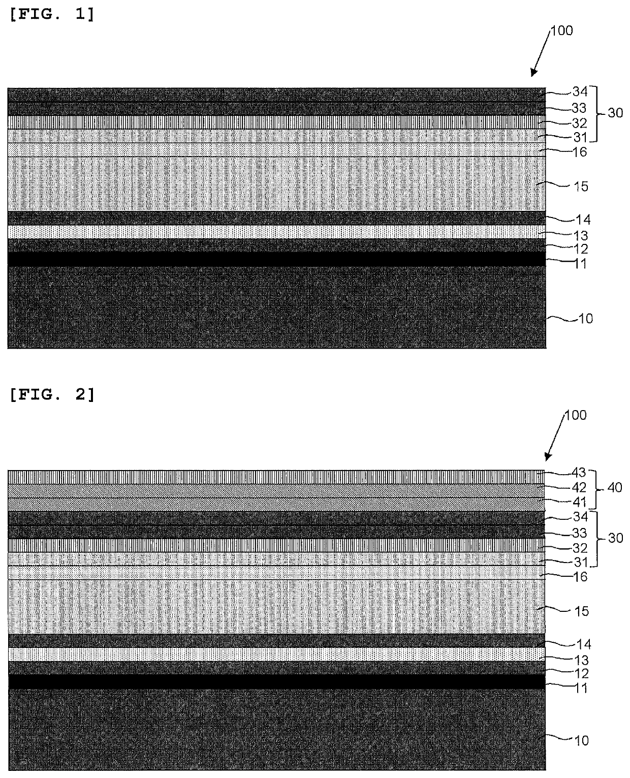
[0054]Firstly, a first wafer having a plurality of independent solar cell structures including a compound semiconductor, the solar cell structures being formed on a starting substrate by epitaxial growth is provided. As described above, the plurality of independent diode circuits and capacitor-function laminated portions can be provided in either one of the first wafer or the second wafer. However, here, the description will be given with these provided on the first wafer.

[0055]FIG. 1 shows a schematic view of the first wafer 100. In the first wafer 100, a plurality of solar cell structures are formed on a starting substrate 10 by epitaxial growth.

[0056]More specifically, the solar cell structures can be formed in the following manner, but the solar cell structures can adopt various structures including a compound semiconductor. Firstly, a p-GaAs buffer layer (not shown) with a thickness of 0.5 μm for example, a p-AlAs sacrificial layer 11 with a thickness of 0.3 μm for example, a p...


PUM


Abstract

A method for producing an electronic device having a drive circuit including a solar cell structure, the method including the steps of: having a first wafer having solar cell structures on a starting substrate and a second wafer having drive circuits formed, so that either one of the first wafer or the second wafer has a plurality of independent diode circuits and capacitor-function laminated portions; obtaining a bonded wafer by bonding so that the solar cell structures, the diode circuits, the capacitor-function laminated portions, and the drive circuits are superimposed; wiring; and dicing the bonded wafer; thus creating a method for producing an electronic device including a drive circuit, a solar cell structure, and a capacitor-function portion in one chip and having a suppressed production cost; and such an electronic device.

Description

TECHNICAL FIELD[0001]The present invention relates to: an electronic device; and a method for producing the same.BACKGROUND ART[0002]Electronic devices such as sensors for IoT (Internet of Things) require chips that are compact and that are driven with low power consumption, and are required to be inexpensive. For such electronic devices, it is ideal to provide a power source on the outside to drive various sensors by electric power supplied from outside to achieve stable operation. However, mounting cost required for wiring becomes massive, and inexpensive sensor-mounting becomes difficult. Accordingly, sensors for IoT require the realization of devices that do not need to be wired for a drive power source.[0003]In addition, an electronic device needs to be compact in order to be inexpensive. In order to realize the above conditions, it is necessary to achieve a drive circuit and a drive-power-receiving device in one chip in an electronic device. As a system for obtaining a power s...

Claims


Application Information

Patent Timeline
IPC IPC(8): H01L31/02H01L31/0443H01L31/053H01L31/0735H01L31/18
CPCH01L31/02021H01L31/0443H01L31/186H01L31/0735H01L31/1844H01L31/053H01L21/50H01L24/05H01L25/162H01L27/142H01L2224/05Y02E10/544H01L21/7806H01L31/0304H01L31/0693H01L2224/18H01L25/167H01L31/18
Inventor ISHIZAKI, JUNYA
Owner SHIN-ETSU HANDOTAI CO LTD
Why Eureka
Try Eureka