Method for producing electronic device

Pending Publication Date: 2022-06-02
SHIN-ETSU HANDOTAI CO LTD
View PDF0 Cites 0 Cited by
  • Summary
  • Abstract
  • Description
  • Claims
  • Application Information

AI Technical Summary

Benefits of technology

The invention provides a method for making electronic devices with a small drive circuit area, which can help reduce production costs.

Problems solved by technology

However, mounting cost required for wiring becomes massive, and inexpensive sensor-mounting becomes difficult.
However, microwaves have great output attenuation due to distance, and are not suitable as an electricity supply system for sensors for IoT having a dispersal arrangement.
A power receiving device for optical wireless power receiving is a solar cell, and it is difficult to provide a drive circuit and a power receiving device in one chip.
However, the power receiving efficiency of a Si-based solar cell on which a drive circuit is mounted is not high, and a large area is required.
As a result, it is difficult to fabricate an inexpensive device.
However, if epitaxial growth of a compound semiconductor solar cell on a Si substrate is attempted, lattice mismatch with the Si substrate becomes large.
As a result, it is necessary to devise a buffer layer for epitaxial growth, and so forth in order to raise the quality of the crystal to form a high-efficiency power receiving solar cell, and this leads to a rise in epitaxial cost.
As a result, device production cost becomes high in any case.

Method used


Image

  • Method for producing electronic device
  • Method for producing electronic device
  • Method for producing electronic device

Examples


first embodiment

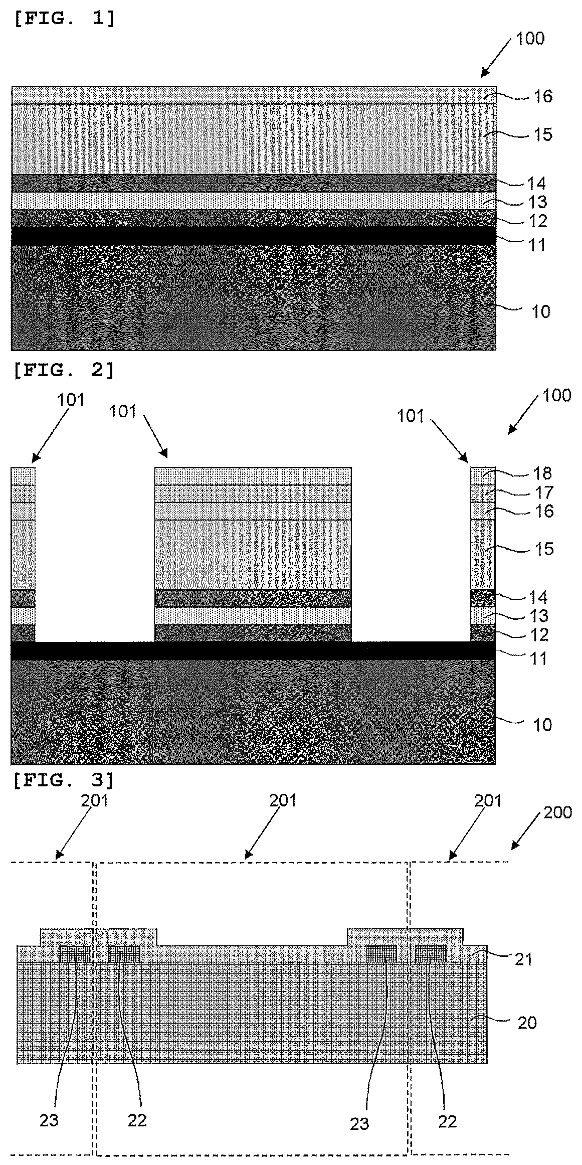
[0046]Firstly, a first wafer having a plurality of independent solar cell structures including a compound semiconductor, the solar cell structures being formed on a starting substrate by epitaxial growth is provided. FIG. 1 and FIG. 2 show schematic views of the first wafer 100. In the first wafer 100, a plurality of solar cell structures 101 are formed on a starting substrate 10 by epitaxial growth.

[0047]More specifically, the solar cell structures can be formed in the following manner, but the solar cell structures can adopt various structures including a compound semiconductor. Firstly, a p-GaAs buffer layer (not shown) with a thickness of 0.5 μm for example, a p-AlAs sacrificial layer 11 with a thickness of 0.3 μm for example, a p-GaAs contact layer 12 with a thickness of 0.3 μm for example, a p-In0.5Ga0.5P window layer 13 with a thickness of 0.2 μm for example, a p-GaAs emitter layer 14 with a thickness of 0.5 μm for example, an n-GaAs base layer 15 with a thickness of 3.5 μm f...

second embodiment

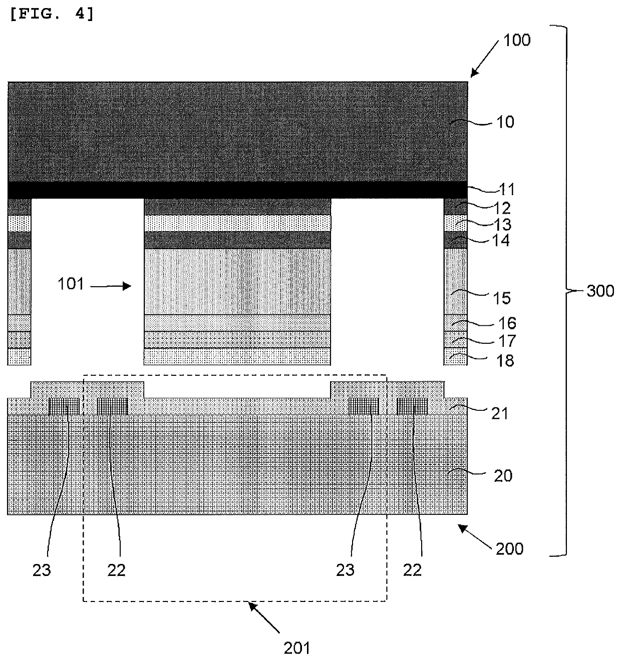
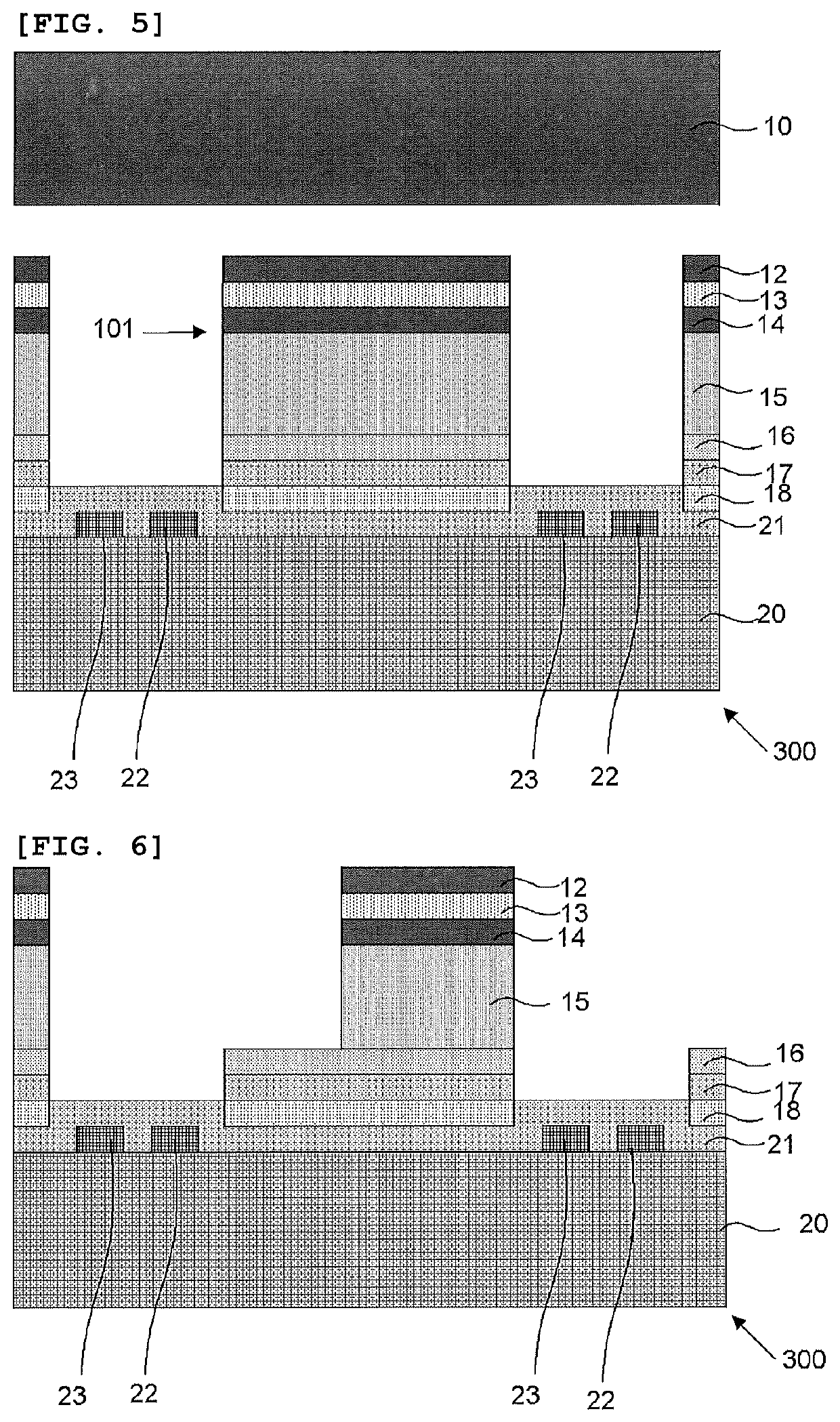
[0071]Next, the second embodiment of the present invention having the steps in the middle of the first embodiment changed will be described. The second embodiment is basically similar to the first embodiment, but is different in the wiring method. The second embodiment is similar to the first embodiment in that pad electrodes 22 and 23 are provided in the second wafer 200 so that electric power can be supplied to drive circuits before carrying out the bonding for an electronic device formed in the second embodiment. However, the second embodiment is different in that an electrode 52 for a solar cell structure is formed in advance before carrying out the bonding so that electric power can be extracted from the solar cell structure of the first wafer (see FIG. 11). In the following, the second embodiment will be described, focusing on differences from the first embodiment. The description will be given using the same reference number for the constituents that are substantially the sam...


PUM


Abstract

The present invention is a method for producing an electronic device having a drive circuit including a solar cell structure, the method including the steps of: obtaining a bonded wafer by bonding a first wafer having a plurality of independent solar cell structures including a compound semiconductor, the solar cell structures being formed on a starting substrate by epitaxial growth, and a second wafer having a plurality of independent drive circuits formed, so that the plurality of solar cell structures and the plurality of drive circuits are respectively superimposed; wiring the bonded wafer so that electric power can be supplied from the plurality of solar cell structures to the plurality of drive circuits respectively; and producing an electronic device having the drive circuit including the solar cell structure by dicing the bonded wafer. This provides a method for producing an electronic device including a drive circuit and a solar cell structure in one chip and having a suppressed production cost.

Description

TECHNICAL FIELD[0001]The present invention relates to a method for producing an electronic device.BACKGROUND ART[0002]Electronic devices such as sensors for IoT (Internet of Things) require chips that are compact and that are driven with low power consumption, and are required to be inexpensive. For such electronic devices, it is ideal to provide a power source on the outside to drive various sensors by electric power supplied from outside to achieve stable operation. However, mounting cost required for wiring becomes massive, and inexpensive sensor-mounting becomes difficult. Accordingly, sensors for IoT require the realization of devices that do not need to be wired for a drive power source.[0003]In addition, an electronic device needs to be compact in order to be inexpensive. In order to realize the above conditions, it is necessary to achieve a drive circuit and a drive-power-receiving device in one chip in an electronic device. As a system for obtaining a power supply wirelessl...

Claims


Application Information

Patent Timeline
IPC IPC(8): H01L25/16H01L31/18H01L23/00H01L31/02
CPCH01L25/167H01L2224/92244H01L31/1892H01L24/29H01L24/83H01L31/02008H01L24/24H01L24/92H01L24/73H01L24/32H01L24/94H01L31/1844H01L2224/245H01L2224/24146H01L2224/2919H01L2224/32145H01L2224/73267H01L2224/73217H01L24/82H01L2224/82106H01L2224/83203H01L2224/83862H01L2224/92144H01L31/1876Y02P70/50H01L24/00H01L21/7806H01L31/0693H01L31/02021H01L27/142H01L31/0735H01L31/184Y02E10/544
Inventor ISHIZAKI, JUNYAFURUYA, SHOGOAKIYAMA, TOMOHIRO
Owner SHIN-ETSU HANDOTAI CO LTD
Why Eureka
Try Eureka