Electronic package and fabrication method thereof

a technology of electronic packaging and fabrication methods, applied in the direction of shielding material radiating elements, independent non-interaction antenna combinations, and semiconductor/solid-state device details, etc., can solve the problems of reducing the width imposing difficulty in meeting the requirements of antenna operation of the 5g system, and hindering the miniaturization of the wireless communication modul

Active Publication Date: 2022-08-18
SILICONWARE PRECISION IND CO LTD
View PDF10 Cites 0 Cited by
  • Summary
  • Abstract
  • Description
  • Claims
  • Application Information

AI Technical Summary

Benefits of technology

The present patent improves the efficiency of antennas in electronic packages by adding recesses that enhance radiation. This leads to better performance and higher electric field intensity, making it easier to transmit signals for 5G networks. The recesses also allow for adjustments in electromagnetic coupling distances, enabling different antenna signals to be transmitted. This reduces the size of electronic packages and eliminates the need for increased layout area, making it easier to fabricate antennas with various frequencies for miniaturized electronic devices.

Problems solved by technology

As such, the wireless communication module 1 cannot provide electrical functions required for operating the 5G system, imposing a difficulty in meeting the requirement of antenna operation of the 5G system.
Consequently, it is difficult to reduce the width of the wireless communication module 1, thus hindering miniaturization of the wireless communication module 1.
Therefore, how to overcome the above-described drawbacks of the prior art has become an urgent issue in the art.

Method used


Image

  • Electronic package and fabrication method thereof
  • Electronic package and fabrication method thereof
  • Electronic package and fabrication method thereof

Examples


Embodiment Construction

[0035]The following illustrative embodiments are provided to illustrate the present disclosure, these and other advantages and effects can be apparent to those in the art after reading this specification.

[0036]It should be noted that all the drawings are not intended to limit the present disclosure. Various modifications and variations can be made without departing from the spirit of the present disclosure. Further, terms such as “first,”“second,”“on,”“a,” etc., are merely for illustrative purposes and should not be construed to limit the scope of the present disclosure.

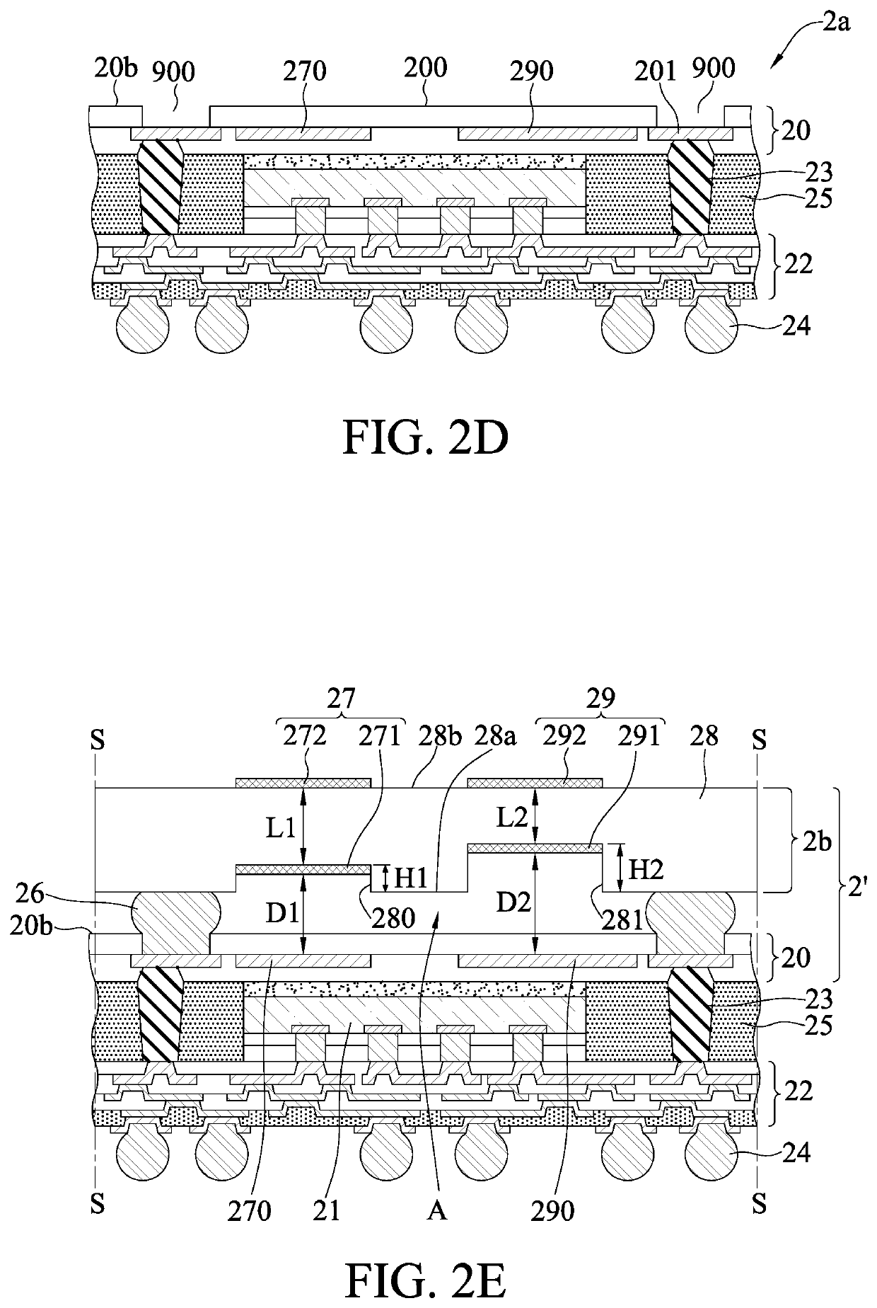
[0037]FIGS. 2A to 2F are schematic cross-sectional views illustrating a method for fabricating an electronic package 2 according to a first embodiment of the present disclosure.

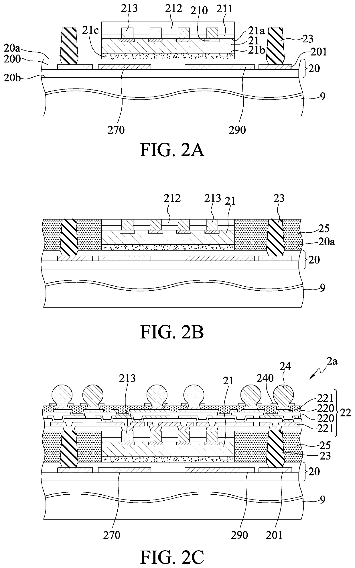
[0038]Referring to FIG. 2A, a first carrier structure 20 having opposite first and second sides 20a, 20b is provided and disposed on a carrier 9 via the second side 20b thereof. Then, a plurality of conductors 23 are formed on the first side 2...


PUM


Abstract

An electronic package is provided and includes a first carrier structure having a plurality of antenna feed lines, and an antenna module disposed on the first carrier structure. The antenna module includes a substrate body having a plurality of recesses with different depths. Further, antenna layers are formed in the plurality of recesses and electromagnetically coupled to the antenna feed lines so as to improve the overall radiation efficiency of the antenna assembly.

Description

BACKGROUND1. Technical Field[0001]The present disclosure relates to electronic packages, and more particularly, to an electronic package having an antenna structure and a fabrication method thereof.2. Description of Related Art[0002]Currently, wireless communication technologies have been widely applied in a variety of consumer electronic products such as mobile phones and tablet computers to facilitate receiving or transmitting of various wireless signals. To facilitate portability of the consumer electronic products and easy access to Internet (e.g., viewing multimedia contents), wireless communication modules are becoming lighter, thinner, shorter and smaller. Therein, patch antennas have been widely applied in wireless communication modules of electronic products due to their advantages of small size, light weight and easy fabrication.[0003]In addition, along with the improvement of image quality of multimedia contents, more and more multimedia data is produced. Accordingly, wir...

Claims


Application Information

Patent Timeline
IPC IPC(8): H01Q1/22H01Q1/24H01Q1/40H01L23/31H01L23/538H01L23/66H01L23/00H01L21/48H01L21/56H01L21/683
CPCH01Q1/2283H01L2224/214H01Q1/40H01L23/3128H01L23/5383H01L23/5386H01L23/5389H01L23/66H01L24/20H01L24/19H01L21/4853H01L21/4857H01L21/565H01L21/568H01L21/6835H01L2221/68372H01L2223/6677H01Q1/246H01Q1/38H01L2224/32225H01L2224/73267H01L2224/92244H01L2224/04105H01L2224/12105H01L2924/15311H01L2225/1035H01L2225/1041H01L2225/1058H01L2224/16227H01L2224/0401H01L2224/97H01L2224/131H01L2224/73204H01L2225/1023H01L2924/15331H01L24/13H01L24/16H01L24/32H01L24/73H01L24/92H01L2224/92125H01L2224/48227H01L2221/68345H01L2221/68359H01Q9/0414H01Q21/28H01L23/49816H01L23/49833H01L2224/83H01L2224/81H01L2924/014H01L2924/00014H01L2224/16225H01L2924/00
Inventor KE, CHUNG-YULAI, CHIA-CHUCHEN, LIANG-PIN
Owner SILICONWARE PRECISION IND CO LTD
Why Eureka
Try Eureka