Eureka AIR delivers breakthrough ideas for toughest innovation challenges, trusted by R&D personnel around the world.

Electric circuit device

Pending Publication Date: 2022-08-18
HITACHI ASTEMO LTD
View PDF0 Cites 0 Cited by
  • Summary
  • Abstract
  • Description
  • Claims
  • Application Information

AI Technical Summary

Benefits of technology

The invention reduces distortion in the inductance loop and improves the reduction of inductance.

Problems solved by technology

In such an electric circuit device having a switching element, there is a possibility that the voltage increases due to self-inductance when the switching element is turned on or off, and a surge-like high voltage is generated.

Method used


Image

  • Electric circuit device
  • Electric circuit device
  • Electric circuit device

Examples


Embodiment Construction

[0020]Embodiments of the present invention will be described below with reference to the accompanying drawings. The following description and drawings are examples for describing the present invention, and are omitted and simplified as appropriate for the sake of clarity of description. The present invention can be carried out in various other forms. Unless otherwise specified, each component may be singular or plural.

[0021]Positions, sizes, shapes, ranges, and the like of the respective components illustrated in the drawings may not represent actual positions, sizes, shapes, ranges, and the like in order to facilitate understanding of the invention. Therefore, the present invention is not necessarily limited to the positions, sizes, shapes, ranges, and the like disclosed in the drawings.

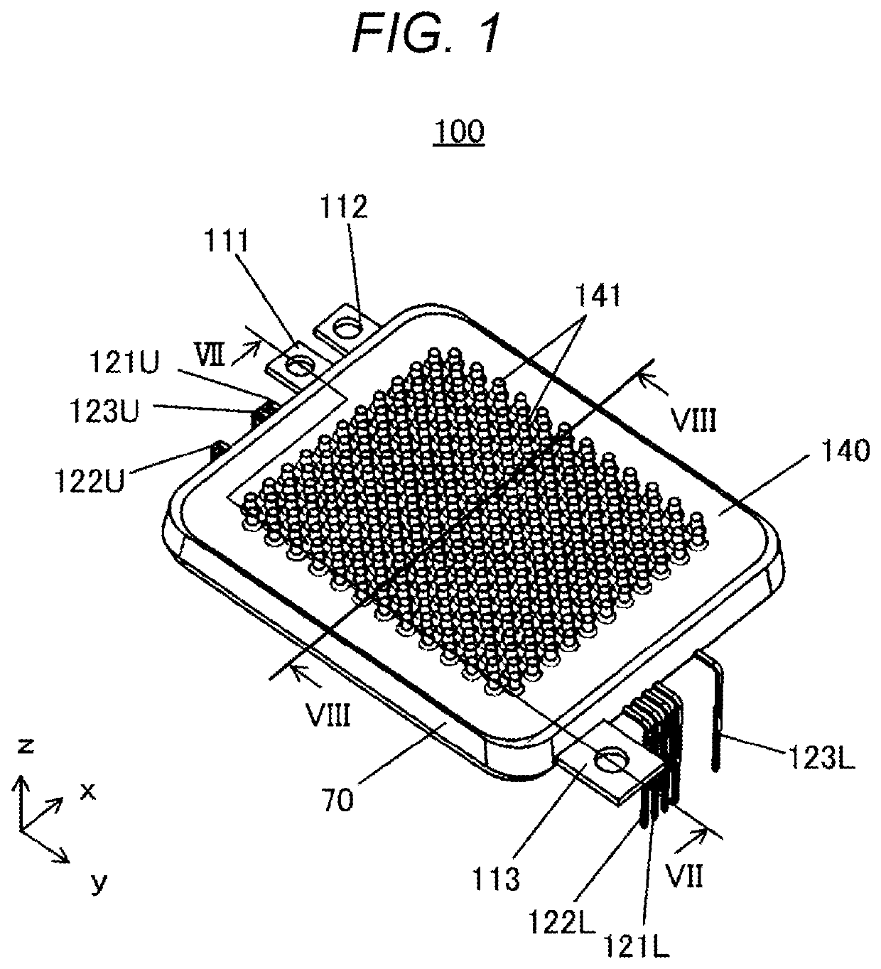
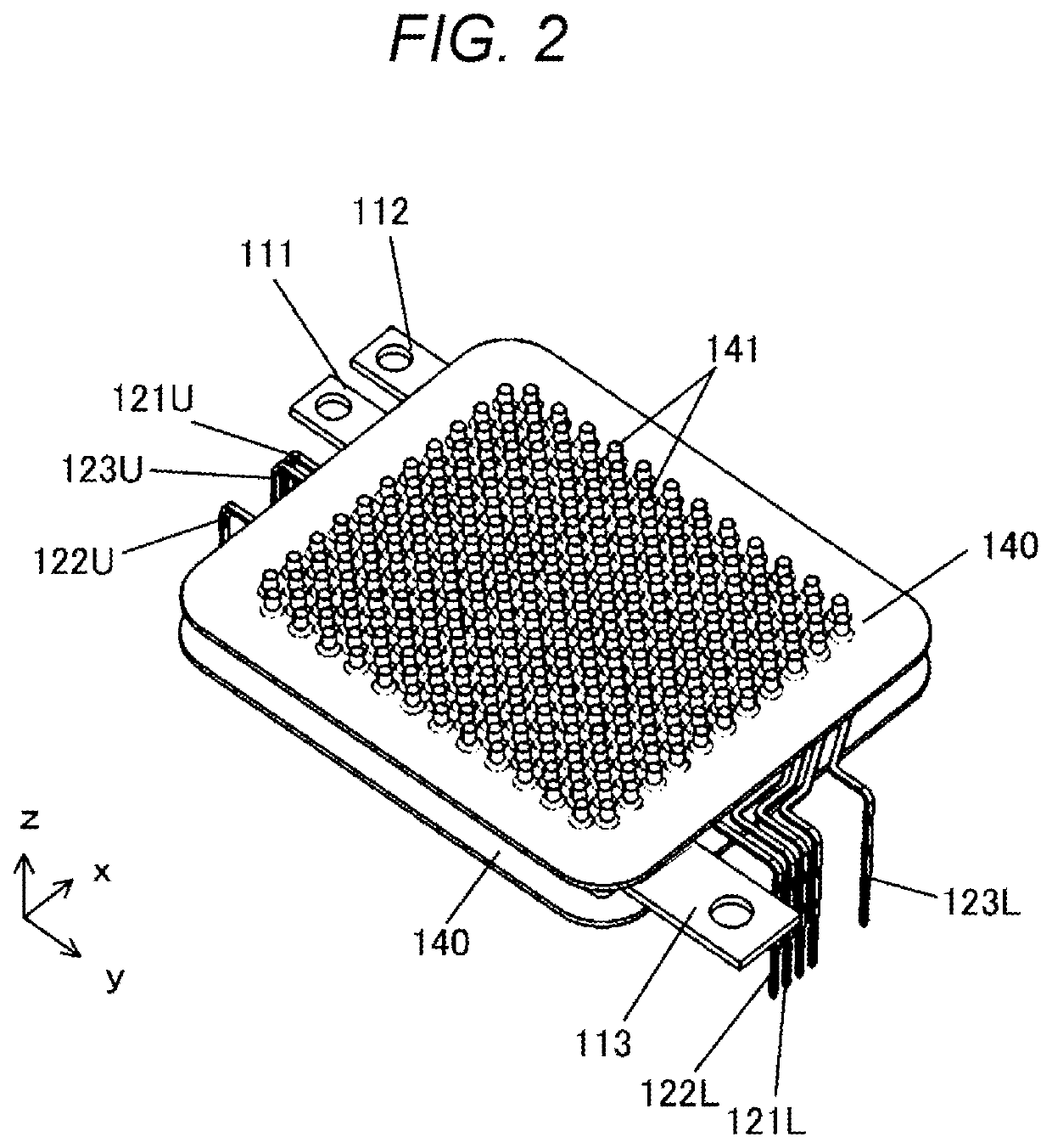
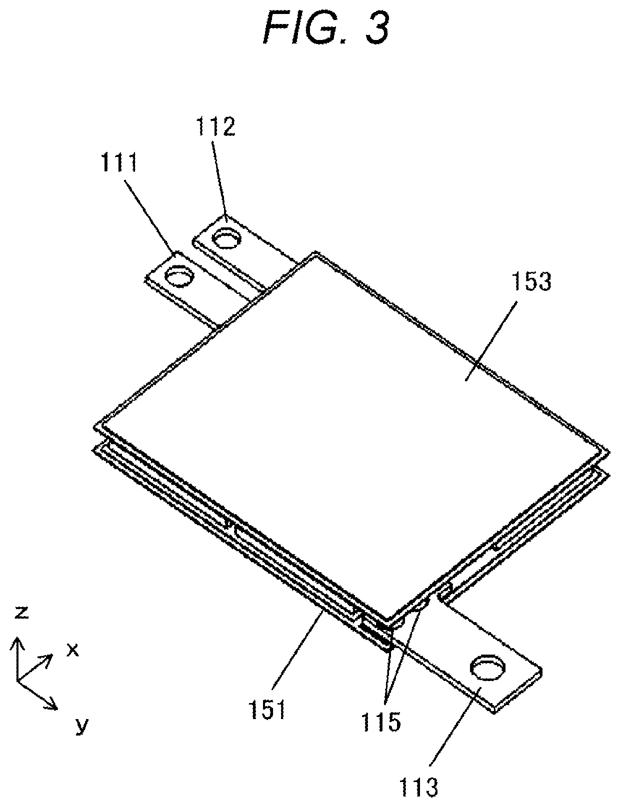
[0022]FIG. 1 is an external perspective view of an embodiment of an electric circuit device according to the present invention. FIG. 2 is a perspective view of the electric circuit device illustrate...


PUM


Abstract

An inductance reduction effect is improved by reducing the distortion of an inductance loop generated when a switching element is turned on and off. An upper arm circuit portion (201U) and a lower arm circuit portion (201L) are provided so as to be shifted in the second direction orthogonal to the first direction in which the upper arm circuit portion (201U) and the lower arm circuit portion (201L) are separated from each other, and at least a part of a snubber circuit connection portion region (202) constituted by a positive electrode terminal portion (181), a negative electrode terminal portion (155), and a snubber element (30) is provided in the first region generated by shifting the upper arm circuit portion (201U) from the lower arm circuit portion (201L) in the second direction.

Description

TECHNICAL FIELD[0001]The present invention relates to an electric circuit device.BACKGROUND ART[0002]Since an electric circuit device such as a power semiconductor module having a power switching element and performing power conversion has high conversion efficiency, the electric circuit device is widely used for consumer use, in-vehicle use, railway use, electric substation equipment, and the like. In such an electric circuit device having a switching element, there is a possibility that the voltage increases due to self-inductance when the switching element is turned on or off, and a surge-like high voltage is generated.[0003]As a structure for suppressing an increase in voltage due to inductance, there is known a power semiconductor module in which a snubber element including a snubber capacitor is disposed between a power switching element and a smoothing capacitor to reduce wiring inductance. As an example of such a power semiconductor module, there is a structure in which an u...

Claims


Application Information

Patent Timeline
IPC IPC(8): H02M7/00H02M1/34H01L23/367
CPCH02M7/003H01L23/367H02M1/34H02M1/00H05K7/209H01L2924/181H01L2224/0603H01L2224/48091H01L2224/33181H01L2224/32225H02M1/327H02M1/348H02M7/538H01L23/3735H01L23/4334H01L2224/48227H01L2224/49113H01L25/072H01L23/5385H01L2924/00012H01L2924/00014
Inventor HAKUTO, TAKUMAOSHIMA, TAKAYUKIMATSUSHITA, AKIRA
Owner HITACHI ASTEMO LTD
Why Eureka
Eureka Blog
Learn More